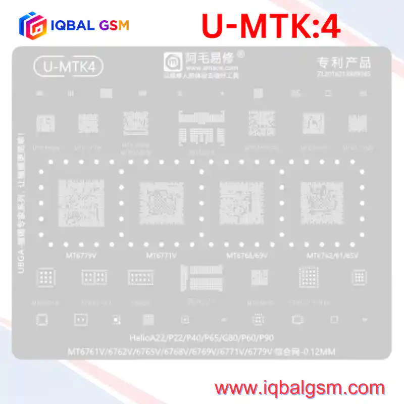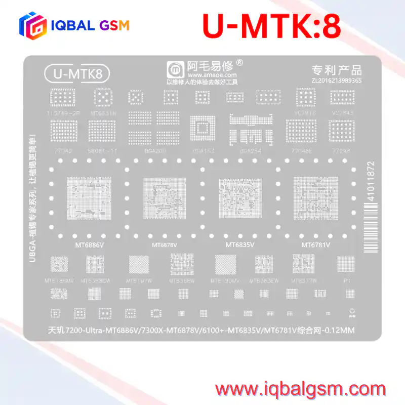

U-MTK 5
As low as
Rs 700.00
Worldwide shipping · Cash on Delivery
Product Details
================================================================================
1. 5G HARDWARE ARCHITECTURE & SILICON TOPOLOGY (DIMENSITY PLATFORM)
================================================================================
The AMAOE U-MTK5 stencil targets MediaTek's Sub-6GHz 5G smartphone ecosystem. Unlike
earlier 4G generations, Dimensity platforms integrate ultra-dense BGA-254 multi-chip memory
and split-phase PMIC architectures:
A. DIMENSITY 5G SoCs (MT6877V / MT6873V / MT6875V / MT6853V / MT6833V):
- Fabrication & Package: TSMC 7nm FinFET (N7) and 6nm (N6).
- Ball Pitch & Substrate: 0.35 mm ultra-fine ball pitch with asymmetric center ground and
bypass capacitor keep-out cutouts.
- Failure Characteristics: Due to the high thermal density of 5G modem processing combined
with heavy CPU/GPU loads, these SoCs develop solder joint fractures around the outer corner
ground arrays and high-speed memory interface lines. Typical symptoms include sudden power-off,
stuck on vendor splash screen (Fastboot loop), or device enumeration in MTK Preloader / BROM mode.
B. BGA-254 uMCP / UFS MEMORY SUBSYSTEM:
- Form Factor: JEDEC BGA-254 (11.5 mm x 13.0 mm, 0.5 mm ball pitch).
- Architecture: Integrates high-speed UFS 2.2 / 3.1 storage and 4-channel 16-bit LPDDR4X /
LPDDR5 memory inside a single multi-chip package.
- Power Rails:
* VCC (3.3V / 2.5V): UFS NAND flash core.
* VCCQ / VCCQ2 (1.8V / 1.2V): UFS logic controller and I/O interface.
* VDD1 (1.8V), VDD2 (1.1V), VDDQ (0.6V): LPDDR4X / LPDDR5 DRAM power rails supplied by MT6359.
- Common Failure: A cracked or cold solder joint on the differential UFS data lines (DIN_T/C, DOUT_T/C)
causes the SoC to drop into USB BROM DFU mode (Hardware ID: 0e8d:0003).
C. POWER DELIVERY ARCHITECTURE (MT6359VNP + MT6360 + MT6315GP):
- Master PMIC (MT6359VNP / MT6359VPW):
* Generates all primary system voltages, baseband modem LDOs, 32.768 kHz RTC clock, and handles
power-on reset (RESETB) sequencing with the Dimensity AP.
- Secondary PMIC / Sub-PMIC (MT6360):
* WLCSP-103 package handling USB Type-C PD negotiation, primary 3A switched battery charging,
USB OTG boost (5V @ 1.5A), display backlight/bias power (VSP / VSN ±5V rails), and flash LED.
* High-Risk Component: Blown MT6360 chips cause severe motherboard heating, zero battery charging,
or dead short to ground on VBAT/VSYS.
- Multiphase Sub-PMIC (MT6315GP):
* Operates in dynamic multi-phase step-down configuration to supply low-voltage, high-current
transients (0.6V - 0.9V @ up to 15A) directly to the MT6877/MT6833 CPU big-core clusters.
D. 5G RF TRANSCEIVERS & HIGH-POWER FRONT-END MODULES:
- MT6190W / MT6190MV: 5G NR Sub-6GHz transceiver interfacing with the baseband over MIPI RFFE.
- VC7920-11 & SKY78191-21: High-power integrated PAMiD modules with large central ground thermal
slugs. Coplanar reballing is essential to prevent RF module tilting and open transmission paths.
================================================================================
2. SOLDER PASTE SELECTION & THERMAL PARAMETERS
================================================================================
- Stencil Thickness: Exactly 0.12 mm laser-cut hardened Japanese stainless steel.
- Solder Paste Alloy:
* Sn63/Pb37 (63% Tin / 37% Lead) Eutectic Alloy (Melting Point: 183°C).
* Mesh Particle Size: Type 4 (20 - 38 microns) or Type 5 (15 - 25 microns) is strictly required
for the dense 0.35 mm pitch of MT6877V and BGA254.
* Flux Formulation: No-Clean / Rosin Mildly Activated (RMA) high-viscosity tacky flux.
- Temperature Profiles:
* Stencil Ball Reflow: 310°C - 325°C hot air, 25% - 30% airflow.
* Board Desoldering: 350°C - 365°C (with bottom preheating plate at 145°C - 160°C).
* Board Installation / Reflow: 335°C - 350°C until self-alignment surface tension is verified.
================================================================================
3. COMPREHENSIVE 5G SoC & BGA-254 REWORK WORKFLOW
================================================================================
STEP 1: PRE-HEATING & CHIP EXTRACTION
1. Mount the logic board in a dedicated CNC/magnetic PCB holder. Mask camera connectors, battery FPCs,
and microphones with double-layer aluminum heat-shielding tape.
2. Bottom Pre-Heat: Apply 150°C across the board underside to eliminate internal multi-layer PCB stress.
3. Apply tacky flux around the perimeter of the target Dimensity SoC (MT6877/MT6833) or BGA254 uMCP.
4. Using an 8 mm or 10 mm circular nozzle on the hot-air station, set temperature to 355°C - 365°C (airflow 45%).
5. Heat in smooth, continuous rectangular motions 1.5 cm above the chip for 35-45 seconds.
6. Verify solder liquefaction by nudging an adjacent surface-mount capacitor. Lift the chip straight
up using precision vacuum tweezers or ultra-fine curved tweezers (#5). Avoid any lateral prying.
STEP 2: PAD RESURFACING & EPOXY REMOVAL
1. Reduce hot air to 250°C and apply RMA flux. Use a specialized copper underfill scraper blade to peel
the softened factory black epoxy underfill from both the PCB and the IC margins.
2. Tin the footprint pads with 183°C leaded solder using a 330°C iron (C210 bevel/knife tip).
3. Place high-purity copper desoldering wick across the pads and glide the flat iron face across the
wick without applying downward pressure.
4. Clean with 99.9% IPA until all pads are completely planar and mirror-smooth. Inspect under 30x
microscope magnification to ensure no mask blistering or torn copper traces.
STEP 3: REBALLING WITH THE AMAOE U-MTK5 STENCIL
1. Seat the cleaned IC into a magnetic reballing fixture.
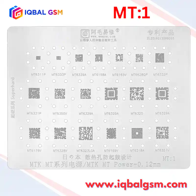
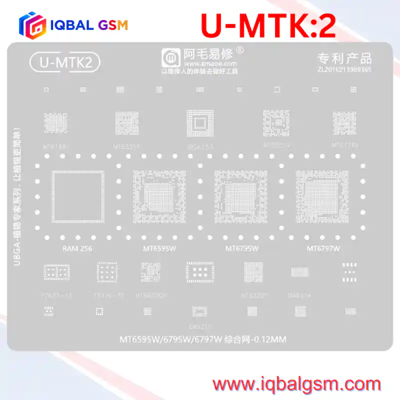
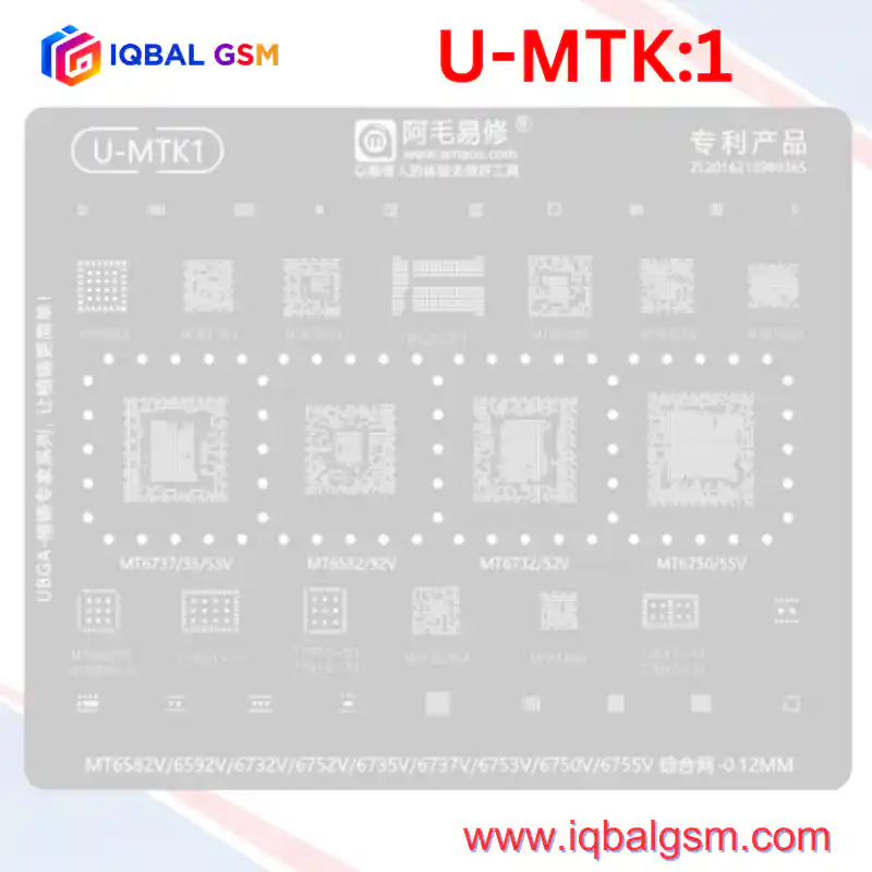
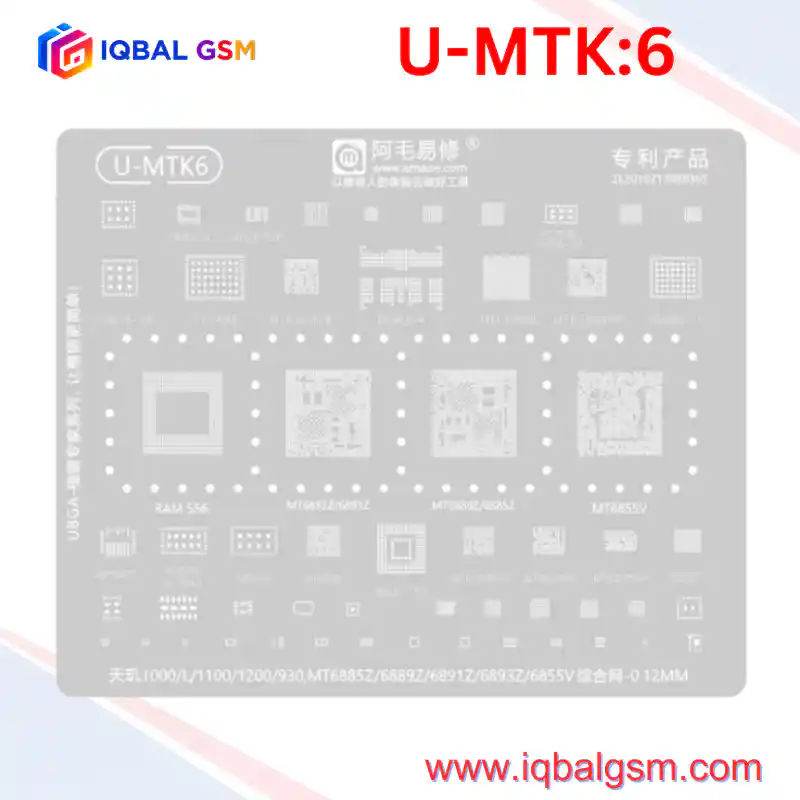
2. Position the corresponding aperture on the U-MTK5 stencil (e.g., MT6877V, MT6833V, BGA254, or MT6359).
Ensure the circular heat-expansion vents surround the chip boundaries to prevent thermal bulging.
3. Apply dry-consistency Sn63/Pb37 solder paste to a flexible steel spatula.
4. Spread the paste into the apertures at a 45° angle, packing each via completely. Wipe the stencil
face clean of any excess solder beads.
5. Hold the stencil down firmly with bent titanium tweezers.
6. Direct hot air at 310°C - 325°C (airflow 25% - 30%) 3 cm above the stencil, circling inward.
Observe the paste coalesce into uniform spheres across all rows.
7. Allow 10 seconds for cooling before lifting the stencil vertically.
8. Apply a drop of liquid flux and pass hot air for 3 seconds at 300°C to allow all balls to reflow
into perfectly symmetrical, centered BGA spheres.
STEP 4: MOTHERBOARD INSTALLATION
1. Spread a micro-thin layer of tacky flux across the PCB pads (shiny, not flooded).
2. Align the IC with the PCB silkscreen corner brackets (verify Pin 1 dot orientation).
3. Reflow with hot air at 340°C - 350°C (airflow 40%). When the solder melts, surface tension will pull
the IC into exact alignment. Give a gentle 0.1 mm tweezer nudge: the chip must snap back immediately.
================================================================================
4. ELECTRICAL DIAGNOSTICS & BOOT-LOOP FAULT MATRIX
================================================================================
1. Diode-Mode Impedance Verification (Unpowered board, Red probe to GND, Black probe to test point):
- VPROC / VCORE Coils (MT6359 / MT6315) : 0.018 V - 0.065 V (Normal low-impedance buck loop).
- VIO18 / VCCQ (1.8V System I/O) : 0.380 V - 0.490 V (Short indicates PMIC or CPU bridge).
- VCC (3.3V UFS NAND Core Supply) : 0.410 V - 0.520 V.
- VSYS / VBAT (Primary Battery Rail) : 0.420 V - 0.540 V (Short < 0.050 V indicates blown MT6360 FET).
2. DC Power Supply Current Signatures (4.0V VBAT Input):
- 0.000 A Standby: Normal prior to pressing Power button.
- 15 mA - 80 mA Leakage (Pre-Power): Blown high-side buck MOSFET inside MT6360 or shorted TVS diode.
- Press Power -> Fixed 35 mA - 55 mA: MT6359 has powered on, but 26 MHz / 32.768 kHz clock is missing,
or the SoC is not releasing RESETB.
- Press Power -> Cycles 70 mA -> 130 mA -> Drops to 0 mA (Bootloop / BROM mode): Dimensity SoC has booted,
but BGA-254 uMCP storage is open, unpowered, or missing firmware communication. Reball the BGA-254.
- Normal Boot Progression: Steps steadily from 90 mA -> 280 mA -> 600 mA -> 1.2 A+ into Android OS.