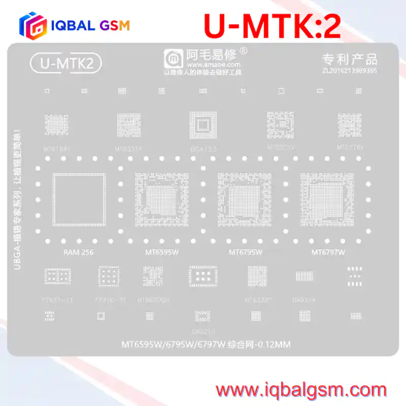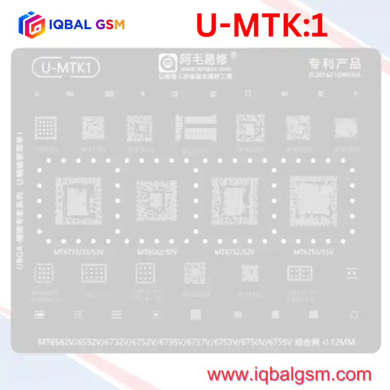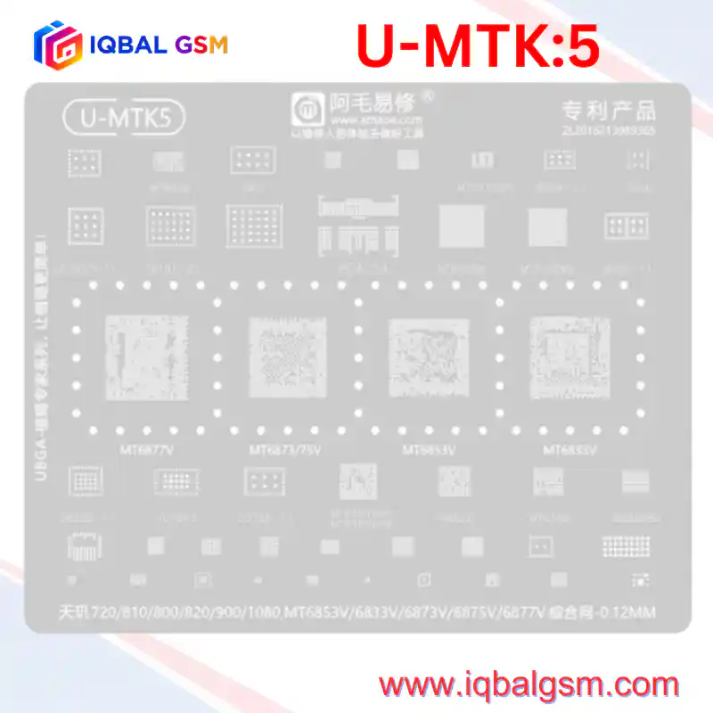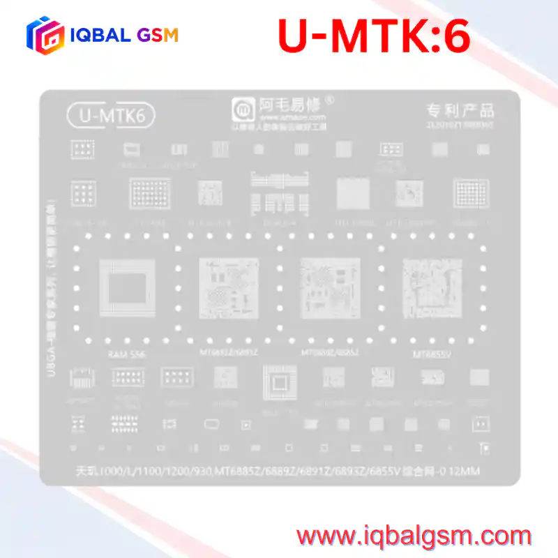

MT-1
As low as
Rs 700.00
Worldwide shipping · Cash on Delivery
Product Details
================================================================================
1. CHIP ARCHITECTURE & POWER-TREE PINOUT ANALYSIS
================================================================================
The AMAOE MT:1 stencil focuses on MediaTek's modular power delivery and RF subsystem,
where power distribution is split across a Master PMIC and dedicated Sub-PMICs:
A. MT6328V/A (VFBGA-206 PACKAGE — 6.6 mm x 6.6 mm):
- Package Architecture: 206-ball Fine-Pitch BGA with outer power rails and inner analog/GND matrix.
- Core Switching Regulators (Buck Converters):
* VPROC (Balls A7, B7, B8, C7, D7): Main CPU core voltage (0.7V - 1.35V dynamic DVS).
* VCORE1 (Balls A5, A6, B5): System interconnect and GPU logic rail (1.05V).
* VLTE (Balls A12, B12, C12): Dedicated modem baseband processor power.
* VSYS22 (Balls A2, B2): 2.2V intermediate supply for internal high-efficiency LDOs.
* VPA (Balls A15): Multimode RF Power Amplifier supply (0.5V - 3.4V tracker rail).
- Key Linear Regulators (28 Internal LDOs):
* VIO18 (Ball F2): 1.8V Digital I/O rail — mandatory boot requirement for eMMC/UFS and PMIC SPI.
* VIO28 (Ball K2): 2.8V Peripheral rail.
* VTCXO_0 / VTCXO_1 (Balls P9, T16): Ultra-low-noise 2.8V reference supply for 26 MHz crystal oscillator.
* VEMC_3V3 (Ball R10): eMMC NAND core supply (3.3V).
* VMCH / VMC (Balls R9, K4): MicroSD and eMMC I/O power.
* VRF18_0 / VRF18_1 (Balls F10, F9): 1.8V power to MT6169V / MT6176V transceivers.
- Integrated Mixed-Signal Subsystems:
* Full uplink/downlink stereo audio CODEC with direct class-AB/D speaker driver (SPK_P/N, Balls F16/E16).
* 32.768 kHz RTC clock oscillator (Balls T6/R6) maintaining clock without main battery.
* USB BC1.1/1.2 battery detection and switched charging control.
B. DUAL-PMIC TOPOLOGY: MT6331P (MASTER) + MT6332P (SLAVE):
- Used in high-power multi-core platforms (e.g., Helio X10 / MT6795).
- MT6331P: Controls main system sequencing, RTC, audio CODEC, baseband LDOs, and AP reset lines.
- MT6332P: Dedicated slave unit managing high-current dual-phase core buck converter, USB Type-C
Pump Express Plus fast-charging current paths, and high-current camera torch LED drivers.
- Failure Pattern: If MT6332P has an internal short on its high-side MOSFET, the phone will draw
excessive current (> 900 mA) immediately upon connecting DC power, keeping MT6331P from booting.
C. MT6311P (MULTI-PHASE BUCK SUB-PMIC):
- High-density miniature WLCSP/BGA companion IC providing high dynamic current for heavy CPU/GPU loads.
- Controlled entirely by the AP and Master PMIC through high-speed I2C/SPI control lines.
- Common Failure: Cold solder joints cause the phone to freeze or reboot under 3D gaming or camera launch.
D. RF TRANSCEIVERS: MT6169V & MT6176V:
- Direct-conversion transceivers interfacing the baseband modem with front-end modules (FEM).
- Sensitive to heat: Overheating during desoldering causes internal die delamination, resulting in
"No Service", "Emergency Calls Only", or a persistent baseband crash preventing device wake-up.
================================================================================
2. SOLDER PASTE & TEMPERATURE PROFILE SPECIFICATIONS
================================================================================
- Stencil Gauge: 0.12 mm laser-cut stainless steel.
- Solder Paste Alloy:
* Sn63/Pb37 (63% Tin / 37% Lead) Eutectic Alloy: Melting point 183°C.
* Particle Size: Type 4 (20 - 38 microns) or Type 5 (15 - 25 microns) mesh is required due to
the tight 0.40 mm pitch on MT6328V, MT6350V, and MT6311P.
* Flux Chemistry: Rosin Mildly Activated (RMA) or No-Clean high-viscosity paste flux.
- Temperature Guidelines:
* Stencil Reflow Hot Air: 300°C - 320°C, airflow 30% - 35%.
* Board Desoldering Hot Air: 345°C - 360°C (with bottom preheat at 140°C - 150°C).
* Board Installation Hot Air: 335°C - 350°C until self-alignment occurs.
================================================================================
3. CHIP-LEVEL REWORK & REBALLING WORKFLOW
================================================================================
STEP 1: IC REMOVAL
1. Apply a thin layer of tacky flux around the target IC (e.g., MT6328V or MT6350V).
2. Set the bottom preheater to 140°C. With a 6 mm circular nozzle on your hot-air wand:
* Direct hot air at 350°C perpendicular to the chip from a distance of 1.5 cm.
* Move in smooth circular patterns around the perimeter for 25-35 seconds.
3. Test solder melt by gently nudging an adjacent non-critical SMD capacitor.
4. Once molten, lift the IC vertically using vacuum tweezers or ultra-fine curved tweezers (#5).
Do NOT twist or yank the chip, as MediaTek thin-laminate PCBs tear copper pads easily.
STEP 2: PAD RESURFACING & CLEANING
1. Apply generous RMA flux to the PCB footprint.
2. Using a temperature-controlled iron (330°C) with a C210-K or C210-SK bevel/knife tip:
* Flood the pads with 183°C leaded solder to dilute the factory lead-free solder.
* Lay quality copper desoldering wick across the pads and glide the flat face of the iron
across the wick without applying downward pressure.
3. Repeat the wicking process on the bottom of the removed IC until all pads are flat and uniform.
4. Clean the PCB and IC with 99.9% IPA and inspect under the microscope for missing or bridging pads.
STEP 3: REBALLING WITH THE AMAOE MT:1 STENCIL
1. Place the cleaned IC on a silicone magnetic reballing fixture.
2. Overlay the corresponding aperture on the AMAOE MT:1 stencil (e.g., MT6328V or MT6350V).
Verify that all pad holes register cleanly with the IC pads.
3. Apply a small ball of dry-consistency Sn63/Pb37 solder paste onto a stainless steel spatula.
4. Spread the paste evenly into the apertures, pressing firmly to ensure complete filling of all
vias. Use a lint-free wiper to remove 100% of the surface paste residue.
5. Hold the stencil down firmly at the margins with bent tweezers.
6. Apply hot air at 310°C (airflow 30%) starting 3 cm above the stencil and gradually lowering to
1.5 cm. Observe as the paste turns into uniform liquid solder balls.
7. Allow the stencil to cool for 5-8 seconds before releasing tension and lifting vertically.
8. Apply a drop of liquid flux and pass hot air for 3 seconds at 300°C to allow all balls to reflow
into perfectly spherical BGA domes.
STEP 4: IC SOLDERING & BOARD INSTALLATION
1. Spread a micro-thin layer of tacky flux on the PCB footprint (the pads should look shiny, not wet).
2. Align the IC with the PCB silkscreen corner brackets (verify Pin 1 orientation mark).
3. Heat at 340°C (airflow 40%). When the solder melts, surface tension will pull the IC into
precise alignment. Give a gentle 0.1 mm tweezer nudge: if the IC snaps back, the joint is solid.
================================================================================
4. ELECTRICAL DIAGNOSTICS & FAULT MATRIX (MTK POWER BOOT)
================================================================================
1. Diode Mode Resistance Checks (Board unpowered, Red probe to GND, Black probe to test point):
- VCORE1 / VPROC Coils : 0.045 V - 0.120 V (Normal low-impedance buck loop).
- VIO18 (1.8V Rail) : 0.380 V - 0.490 V (Short indicates failed PMIC or eMMC/CPU I/O bridge).
- VBAT / VSYS Rail : 0.420 V - 0.520 V (Short < 0.080 V indicates blown high-side PMIC FET).
- VREF / VTCXO Lines : 0.450 V - 0.610 V.
2. DC Power Supply Boot-Up Signatures (4.0V DC Input on VBAT):
- Standby Leakage:
* 0.000 A (Normal).
* 15 mA - 80 mA prior to power key press: Leakage inside primary PMIC (MT6328 / MT6350).
* Dead Short (> 2.0 A current limit): Blown charging/protection diode or shorted main buck FET.
- Power Button Response:
* 0 mA -> Press Power -> 0 mA: Broken PWRKEY line (check Ball E2 on MT6328) or missing VIO18.
* Press Power -> Climbs to 30 mA - 60 mA and freezes: PMIC has powered on, but the 26 MHz /
32.768 kHz clock is missing, or the AP is not releasing RESETB (Ball D3).
* Press Power -> Jumps to 80 mA - 180 mA and drops to 0 mA immediately: Short on a secondary
LDO line (camera, display, or RF rail) causing PMIC overcurrent shutdown.
* Press Power -> Pulses 60 mA -> 120 mA -> 200 mA -> 600 mA+: Normal MTK SoC boot progression.