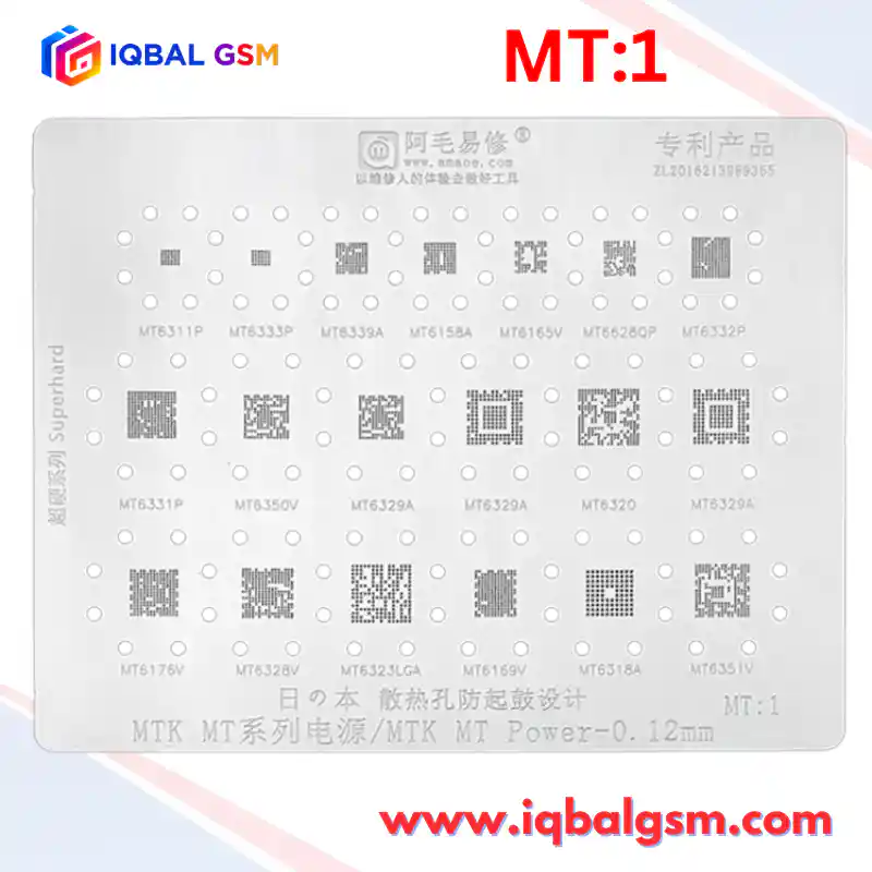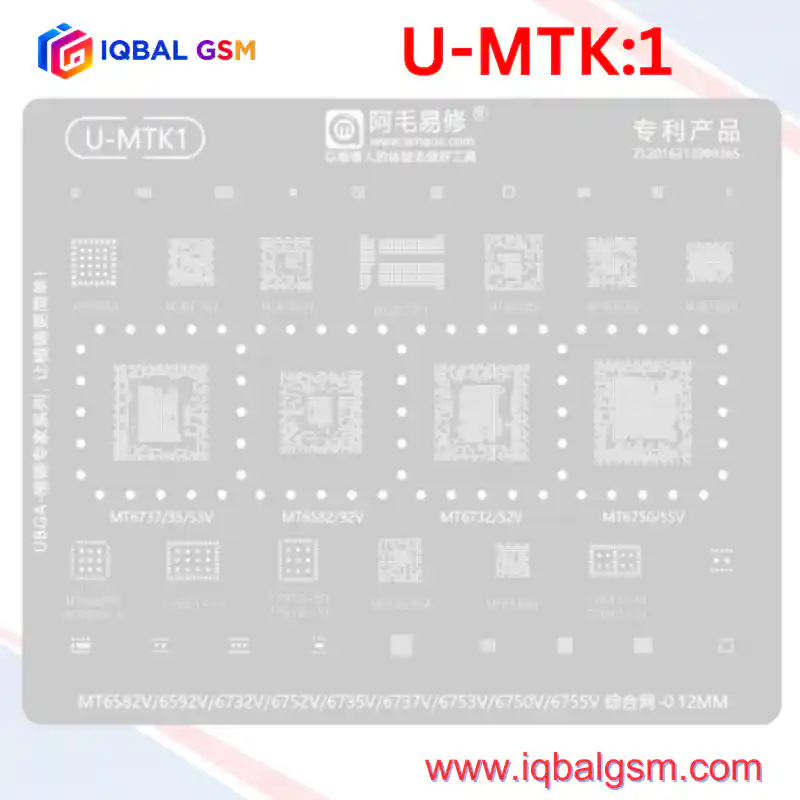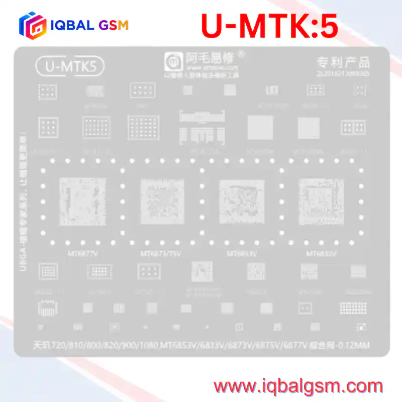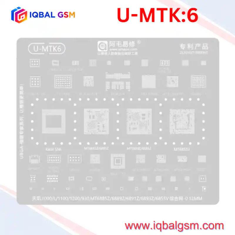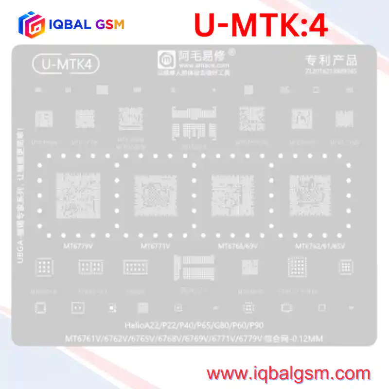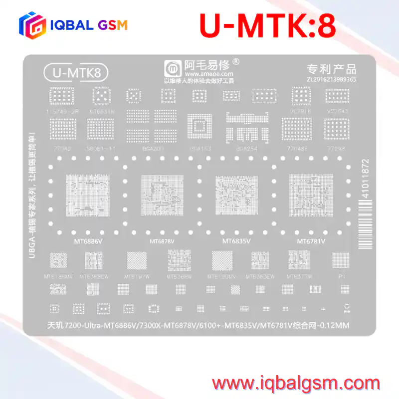

U-MTK 2
As low as
Rs 700.00
Worldwide shipping · Cash on Delivery
Product Details
================================================================================
1. SYSTEM SILICON ARCHITECTURE & POWER-TREE TOPOLOGY
================================================================================
The AMAOE U-MTK2 template addresses the thermal and electrical complexity of MediaTek's
first flagship 20nm/28nm high-power application processors and their companion split-rail power nets:
A. TENSOR / HELIO MULTI-CORE PROCESSORS:
- MT6797W (Helio X20 / X25):
* Tri-Cluster CPU: 2x Cortex-A72 @ 2.3 GHz - 2.5 GHz (Max Performance) + 4x Cortex-A53 @
2.0 GHz (Medium Load) + 4x Cortex-A53 @ 1.4 GHz (Low-Power Efficiency).
* GPU: Arm Mali-T880 MP4 @ 780 MHz.
* Thermal Behavior: Under sustained thermal dissipation, thermal expansion between the 20nm
silicon die and the BT-resin substrate causes center solder ball micro-fractures on VDD_CPU
and VDD_GPU rails, causing sudden reboots, bootlooping at the vendor logo, or a completely dead board.
- MT6795W (Helio X10):
* 28nm HPM process with 8x Cortex-A53 cores running up to 2.2 GHz with PowerVR G6200 GPU.
* Uses the 256-ball Package-on-Package (PoP) upper interposer ring for LPDDR3 memory mounting.
B. SPLIT-POWER DELIVERY: MT6351V / MT6331P / MT6332P / DA9214:
- Master PMIC (MT6351V / MT6331P):
* Generates baseband reference voltages, digital I/O rails (VIO18: 1.8V), analog supply
(VAUD28: 2.8V), 32.768 kHz RTC clock, and manages power-on reset sequencing.
- Slave PMIC (MT6332P):
* Takes the brunt of battery current from the charging port (supporting 15W-18W Pump Express Plus).
* Directly powers auxiliary core buck phases. Common failure point: internal high-side buck MOSFET
shorts drain-to-source, clamping VBAT to ground.
- Dialog DA9214 Sub-PMIC:
* High-frequency dual-phase synchronous step-down converter providing up to 20A dynamic current
specifically for the dual Cortex-A72 cluster. If DA9214 is unseated or cold-soldered, the device
will power on but crash instantly when high CPU clock states are engaged.
C. WIRELESS & RF SUBSYSTEM:
- MT6630QP: Highly integrated 5-in-1 combo chip requiring clean, coplanar solder joints to prevent
Wi-Fi 5 GHz signal degradation or GPS fix dropouts.
- SKY77643-11 & SKY77916-31: High-density RF Power Amplifier modules with central ground thermal pads.
Excessive paste under the center pad causes the module to tilt, leading to perimeter open circuits.
================================================================================
2. SOLDER PASTE & ALLOY SELECTION SPECIFICATIONS
================================================================================
- Stencil Thickness: 0.12 mm precision laser-cut Japanese steel.
- Alloy Hierarchy (Dual-Temperature Rule for PoP Rework):
* Bottom SoC Layer (MT6797W / MT6795W / MT6595W to Motherboard):
- Alloy: Sn63/Pb37 Leaded Solder Paste (Melting Point: 183°C).
- Particle Mesh: Type 4 (20 - 38 microns) or Type 5 (15 - 25 microns).
* Top RAM Layer (RAM 256 onto MT6795W/MT6797W Interposer):
- Alloy: Sn42/Bi58 Low-Temperature Alloy (Melting Point: 138°C) or Sn62/Pb36/Ag2 (179°C).
- Rationale: The upper RAM reflow temperature (230°C - 240°C air) must not reach the 183°C
melting point of the lower SoC balls, preventing bridging and inter-ball solder squish.
* Peripheral PMICs & RF (MT6351V, DA9214, SKY77643-11):
- Alloy: Sn63/Pb37 (183°C).
================================================================================
3. CHIP-LEVEL REBALLING & REWORK PROCEDURE
================================================================================
PHASE 1: DESOLDERING & POP STACK SEPARATION
1. Secure the board in a dedicated motherboard fixture. Place thermal tape over cameras and plastic slots.
2. Bottom Pre-Heat: 150°C across the bottom of the PCB.
3. Top Air: Set hot-air wand to 350°C - 365°C with an 8 mm circular nozzle (airflow 45%).
4. Heat the RAM 256 perimeter uniformly for 30 seconds. Slide a 0.06 mm separation blade between
the RAM and CPU to slice the corner epoxy and lift the RAM off without exerting downward pressure.
5. Reheat the lower SoC (MT6797W/MT6795W) to 365°C and lift vertically with vacuum or fine tweezers.
PHASE 2: RESURFACING & UNDERFILL CLEANING
1. Lower hot air to 250°C and apply RMA flux. Use a copper scraper blade to peel softened black underfill
from both the PCB landing pads and the chip base.
2. Add leaded 183°C solder to the pads with a 330°C iron (C210 bevel tip) to lower the melting point.
3. Level all pads using desoldering wick until coplanar and mirror-smooth. Clean with 99.9% IPA.
PHASE 3: REBALLING WITH AMAOE U-MTK2
1. Position the cleaned IC into the matching aperture on the U-MTK2 stencil:
- For MT6797W, align with the marked Deca-Core matrix.
- For RAM, align with aperture "RAM 256".
- For PMIC/RF, align with MT6331P, MT6332P, MT6351V, DA9214, or MT6169V.
2. Ensure the circular expansion relief vents surround the IC edges to prevent heat bulging.
3. Apply Sn63/Pb37 solder paste with a flexible steel blade at a 45° angle. Scrape off all surface excess.
4. Hot Air Reflow:
- Direct hot air at 310°C - 325°C (airflow 30%) from 3 cm away, circling inward.
- Solder paste coalesces into uniform balls across all apertures.
- Cool for 10 seconds before lifting the stencil vertically.
- Apply a drop of liquid flux and pass hot air for 3 seconds at 300°C for final sphere centering.
PHASE 4: TWO-STAGE INSTALLATION
1. Stage 1 (Base SoC to PCB):
- Apply a microscopic layer of tacky flux to the PCB pads.
- Align the SoC to the silkscreen corner brackets. Reflow at 345°C - 355°C (bottom preheat at 150°C).
- Once surface tension aligns the SoC, perform a gentle 0.1 mm tweezer nudge test to verify all balls
have collapsed and bonded.
2. Stage 2 (RAM 256 to SoC):
- Cool the board completely. Apply a micro-layer of flux to the top interposer ring of the SoC.
- Align the reballed RAM 256 (Pin 1 orientation matched).
- Reflow at 250°C (if using 138°C low-melt paste) or 310°C (if using 179°C paste) with low air (25%).
================================================================================
4. ELECTRICAL DIAGNOSTICS & FAULT MATRIX
================================================================================
1. Diode Mode Impedance Values (Red probe to Ground, Black probe to test point):
- VCORE / VPROC (Main CPU Core Inductors) : 0.025 V - 0.080 V (Normal low-impedance buck loop).
- VIO18 (1.8V System I/O Rail) : 0.380 V - 0.480 V (Short indicates bridged PMIC or CPU ball).
- VBAT / VSYS Rail : 0.420 V - 0.540 V (Short < 0.050 V indicates blown MT6332P FET).
- LPDDR RAM VDD1 / VDD2 : 0.280 V - 0.410 V.
2. DC Power Supply Boot Signatures (4.0V VBAT Input):
- 0.000 A Standby: Normal prior to pressing Power button.
- Fixed 35 mA - 60 mA Current: MT6331P/MT6351V has initiated, but the 26 MHz system clock is absent,
or the CPU is not responding to RESET release.
- Jumping 80 mA -> 160 mA -> Drops to 0 mA: RAM 256 open/bridged joint or corrupt eMMC BGA153 bootloader.
- Immediate Overcurrent (> 1.5 A on connection): Shorted MT6332P, DA9214, or damaged primary power inductor.
- Steps 100 mA -> 280 mA -> 650 mA -> 1.2 A+: Successful boot into Android OS.