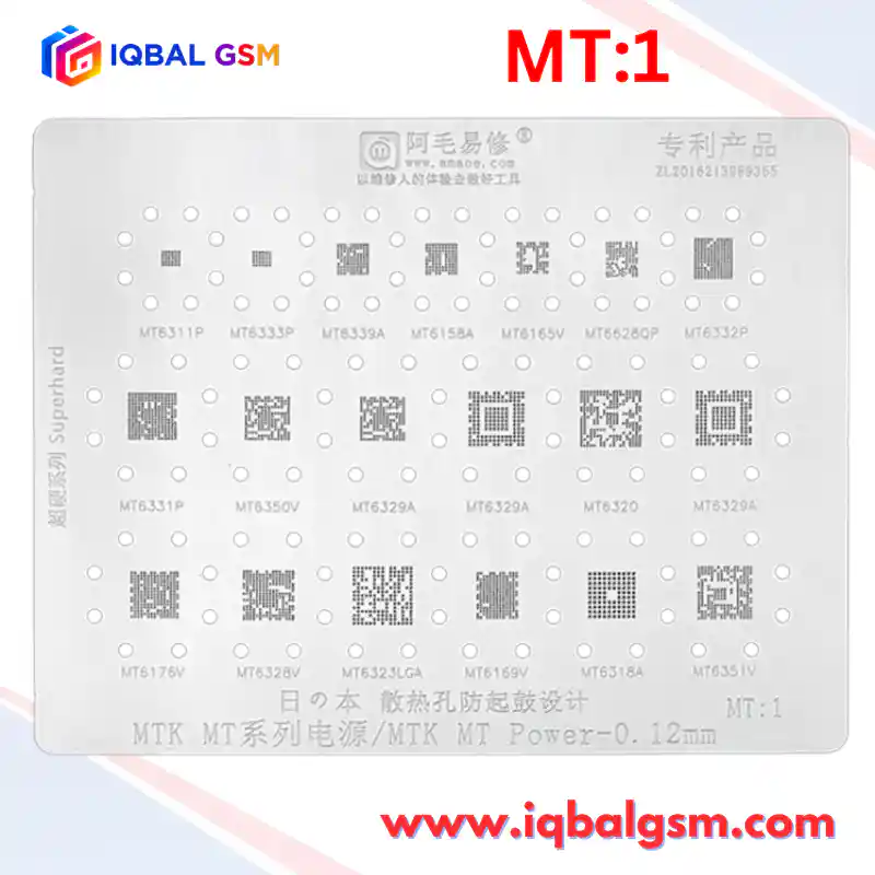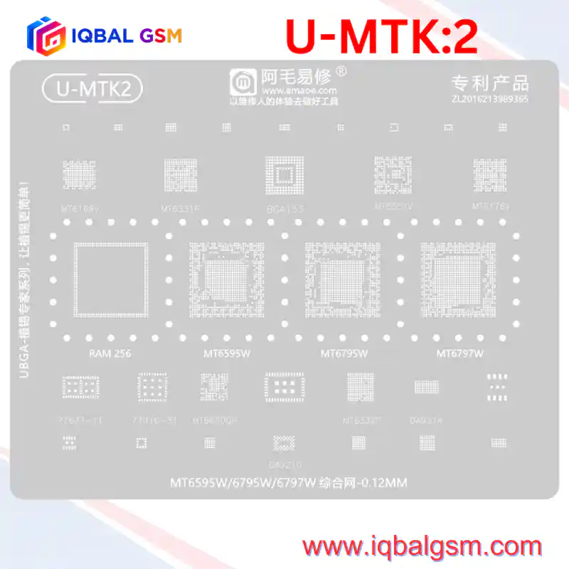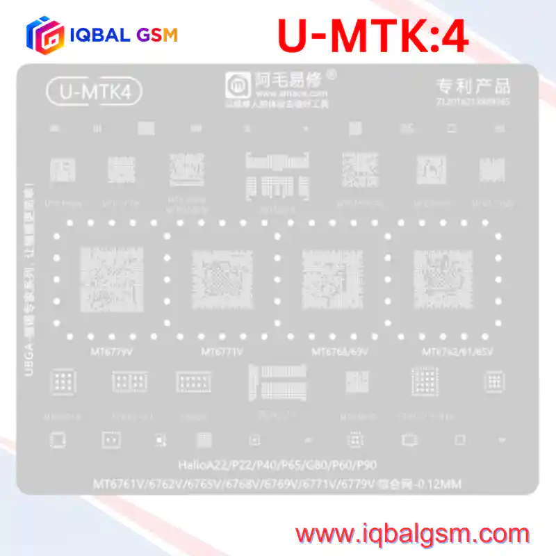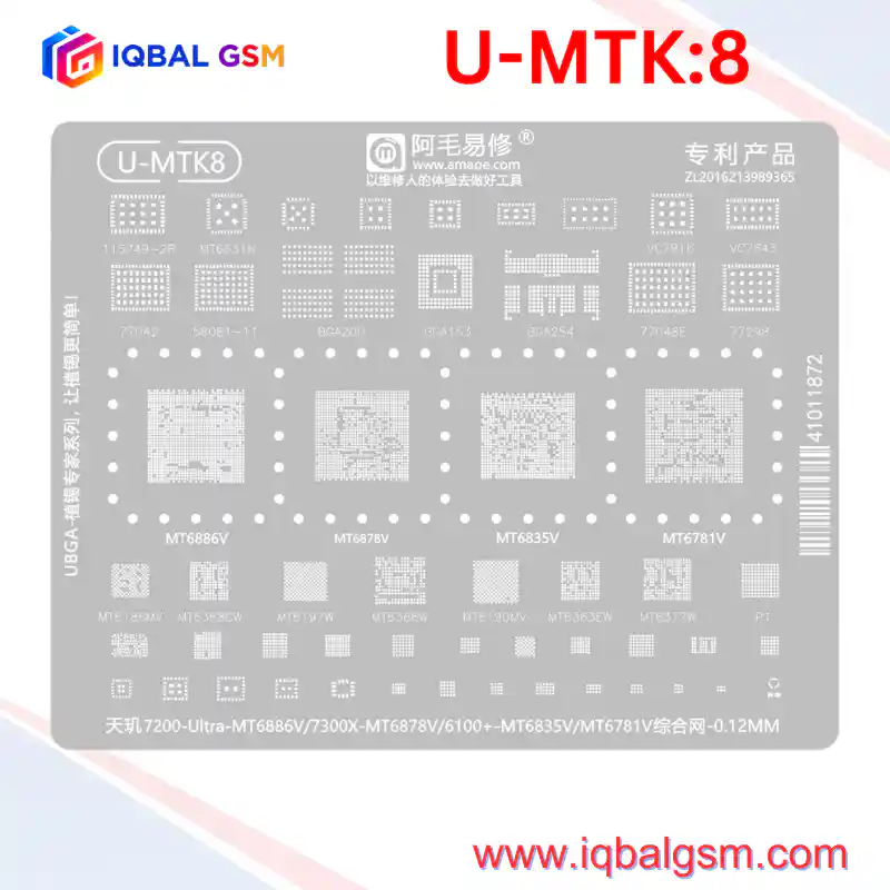

U-MTK 1
As low as
Rs 700.00
Worldwide shipping · Cash on Delivery
Product Details
================================================================================
1. SYSTEM SILICON ARCHITECTURE & PCB DESIGN ANALYSIS
================================================================================
The AMAOE U-MTK1 (151) is the definitive hardware repair stencil for MediaTek's
highest-volume 28nm/40nm mid-range smartphone generation, featuring discrete eMCP
storage architectures rather than top-stacked Package-on-Package (PoP) memory:
A. APPLICATION PROCESSORS (MIDDLE ROW):
- MT6750V / MT6755V (Helio P10):
* Octa-core ARM Cortex-A53 up to 2.0 GHz with Mali-T860 MP2 GPU.
* High thermal cycling stress: Solder micro-fractures frequently develop around the
corner ground balls and inner VCORE buck pads, leading to bootloops or hanging at the logo.
- MT6737V / MT6735V / MT6753V:
* Highly integrated quad-core/octa-core Cortex-A53 64-bit SoCs with direct baseband integration.
* Shares unified BGA layout with varying internal die pad assignments across the series.
- MT6582V / MT6592V:
* Legacy high-density 32-bit quad/octa Cortex-A7 platforms with dense analog periphery lines.
B. BGA-221 eMCP STORAGE ARCHITECTURE:
- Package Standard: JEDEC BGA-221 (11.5 mm x 13.0 mm, 0.5 mm pitch).
- Multi-Chip Construction: Integrates high-speed eMMC 5.1 Flash NAND and LPDDR3 mobile SDRAM
inside a single molded epoxy package.
- Critical Pinout Groups:
* Outer Pad Perimeter: LPDDR3 memory bus lines (DQ0-DQ31, CA0-CA9, CLK, CKE, CS, VDD1/VDD2).
* Center Pad Array: eMMC control bus (CMD, CLK, DAT0-DAT7, VCC 3.3V, VCCQ 1.8V, RST_n).
- Repair Significance: If a device exhibits 80 mA - 120 mA jumping current without display,
reballing the BGA-221 chip resolves loose memory bus solder joints.
C. POWER DELIVERY (MT6328V, MT6351V, MT6323GA):
- MT6328V (VFBGA-206, 6.6 mm x 6.6 mm):
* Powers MT6735, MT6737, MT6750, and MT6755 platforms. Contains 5 buck regulators and 28 LDOs.
* Supplies VPROC (CPU core), VCORE1 (GPU/logic), VLTE (modem), VIO18 (1.8V), and VTCXO (2.8V).
- MT6323GA:
* Powers legacy MT6582/MT6592 platforms via VPROC, VCORE, VIO, and VMC supplies.
D. RF FRONT-END & POWER AMPLIFIERS:
- MT6169V / MT6176V: Direct-conversion multi-band transceivers.
- SKY77621-11 / SKY77645-11 / SKY77916-11: Skyworks PAM modules featuring exposed center
ground slugs. Uneven solder leveling beneath the thermal slug causes module tilting and open RF lines.
================================================================================
2. THERMAL GRADIENTS & SOLDER PASTE SPECIFICATIONS
================================================================================
- Stencil Thickness: 0.12 mm precision laser-cut Japanese stainless steel.
- Solder Paste Alloy:
* Sn63/Pb37 (63% Tin / 37% Lead) Eutectic Alloy: Melting Point 183°C.
* Particle Size: Type 4 (20 - 38 microns) or Type 5 (15 - 25 microns) mesh.
* Flux Formulation: No-Clean / Rosin Mildly Activated (RMA) high-tack flux.
- Working Temperatures:
* Stencil Ball Formation: 300°C - 320°C hot air, 25% - 30% airflow.
* Motherboard Desoldering: 345°C - 360°C (with bottom preheater at 140°C - 150°C).
* Motherboard Reflow / Placement: 335°C - 350°C until self-alignment occurs.
================================================================================
3. STEP-BY-STEP REWORK & REBALLING WORKFLOW
================================================================================
STEP 1: CHIP REMOVAL
1. Secure the motherboard in a high-mass PCB repair fixture. Protect adjacent connectors,
plastic mic ports, and cameras with aluminum foil tape.
2. Preheat the board underside to 140°C - 150°C.
3. Using an 8 mm circular nozzle on the hot-air station, set temperature to 350°C - 360°C (airflow 45%).
4. Heat the target SoC (e.g., MT6750V / MT6737V) or eMCP (BGA-221) in smooth rectangular sweeps
from 1.5 cm above the package for 30-40 seconds.
5. Check solder liquidity by touching an adjacent surface-mount capacitor. Once molten, lift the IC
vertically using fine curved tweezers. Avoid sideways prying to prevent lifting PCB copper pads.
STEP 2: PAD RESURFACING & UNDERFILL REMOVAL
1. Lower hot air to 250°C and apply RMA flux. Gently scrape softened black underfill glue from the
motherboard pads and IC edges using a curved #11 copper blade.
2. Apply fresh 183°C leaded solder to the footprint using a 330°C micro-iron (C210-K bevel tip).
3. Lay high-purity copper wick over the pads and glide the iron across the braid without downward force.
4. Level the IC base pads until smooth and planar. Clean with 99.9% IPA until mirror-clean.
STEP 3: REBALLING WITH THE AMAOE U-MTK1 STENCIL
1. Place the cleaned IC on a magnetic reballing base or silicone mat.
2. Position the corresponding aperture on the U-MTK1 stencil (e.g., MT6750/55V, MT6737/35/53V, or BGA221).
Ensure all pad cutouts register cleanly over the chip pads.
3. Apply a small amount of dry-consistency Sn63/Pb37 solder paste to a flat spatula.
4. Spread the paste into the apertures at a 45° angle, filling all vias. Wipe the stencil face completely
clean of excess paste residue.
5. Hold the stencil down firmly with bent titanium tweezers.
6. Direct hot air at 310°C (airflow 30%) 3 cm above the stencil, lowering gradually. Observe the paste
coalesce into spherical solder balls.
7. Allow 8-10 seconds for cooling, then lift the stencil vertically.
8. Apply a drop of liquid flux and pass hot air for 3 seconds at 300°C to round and center all BGA spheres.
STEP 4: BOARD INSTALLATION
1. Apply a micro-thin layer of tacky flux to the PCB pads (the footprint should look shiny, not flooded).
2. Align the IC with the PCB silkscreen corner brackets (verify Pin 1 dot orientation).
3. Reflow with hot air at 340°C - 350°C (airflow 40%). When the solder liquefies, surface tension will
center the chip. Confirm with a gentle 0.1 mm tweezer nudge test.
================================================================================
4. ELECTRICAL DIAGNOSTICS & FAULT MATRIX
================================================================================
1. Cold Diode-Mode Impedance Verification (Red probe to Ground, Black probe to test points):
- VPROC / VCORE Coils (MT6328 / MT6351) : 0.035 V - 0.110 V (Normal low-impedance buck loop).
- VIO18 (1.8V System I/O Rail) : 0.380 V - 0.490 V (Short indicates PMIC or CPU bridge).
- VCC (3.3V eMCP Flash Core Supply) : 0.420 V - 0.530 V.
- VBAT / Main System Battery Rail : 0.430 V - 0.540 V.
2. DC Power Supply Boot-Up Current Analysis (4.0V DC Input):
- 0.000 A Standby: Normal prior to pressing Power button.
- 15 mA - 80 mA Leakage (Pre-Power): Blown high-side buck MOSFET inside MT6328V or shorted diode.
- Press Power -> Fixed 30 mA - 50 mA: PMIC has initialized, but the 26 MHz crystal oscillator is inactive,
or RESETB is held low by the CPU.
- Press Power -> 80 mA - 140 mA (Cycling / Stalling): CPU has initialized; eMCP BGA-221 storage is
unseated, missing VCC/VCCQ, or has corrupted preloader firmware. Reball or replace BGA-221.
- Normal Boot: Steps steadily from 90 mA -> 250 mA -> 550 mA -> 1.1 A+ into Android OS.