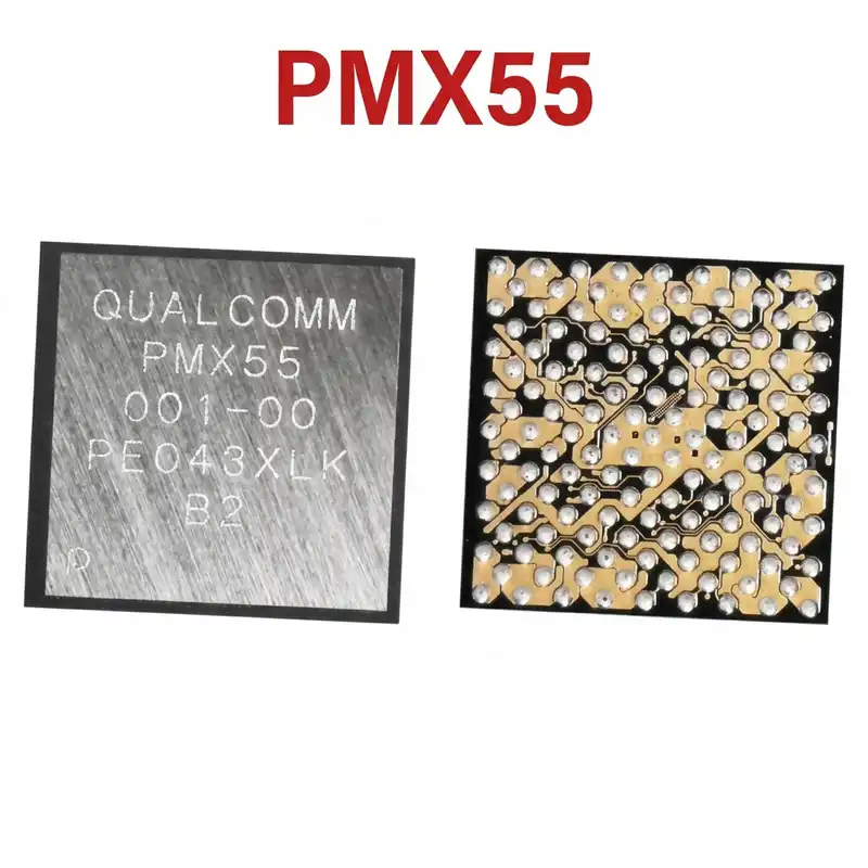
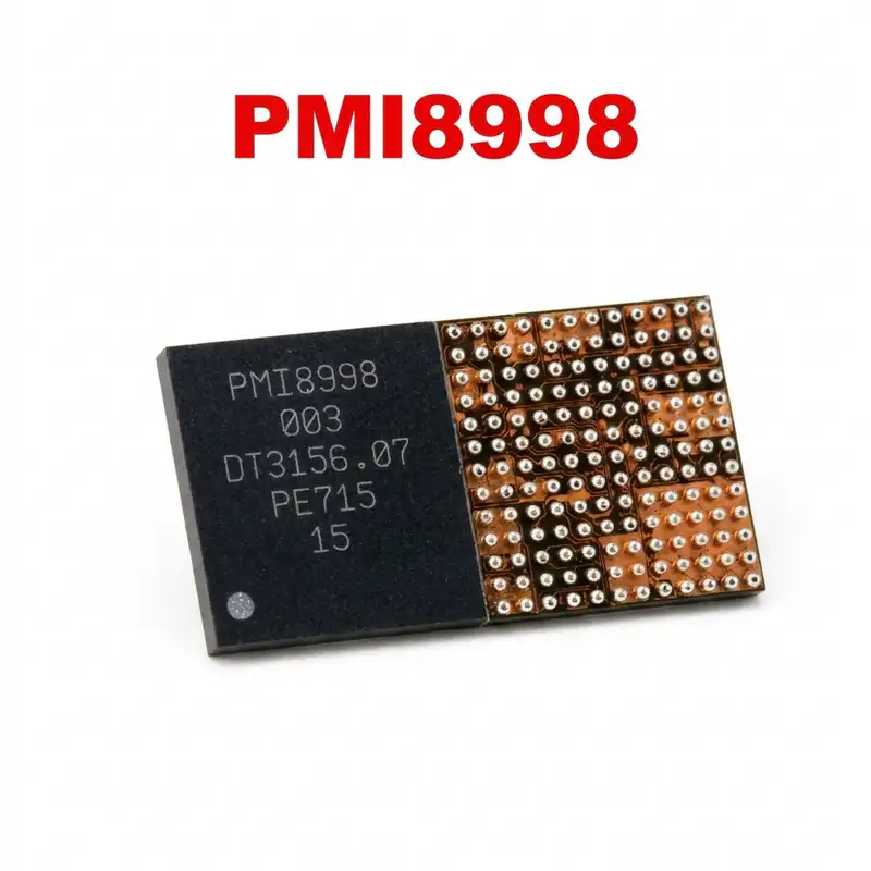
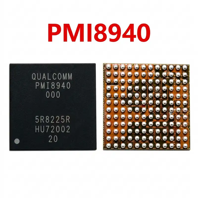
PM670A
As low as
Rs 0.00
Worldwide shipping · Cash on Delivery
Product Details
====================================================================================================
QUALCOMM PM670A (000-01 / 001) POWER MANAGEMENT IC REPAIR & REWORK GUIDE
====================================================================================================
1. PRODUCT IDENTIFICATION & SPECIFICATIONS:
----------------------------------------------------------------------------------------------------
- Part Numbers: PM670A, PM670A-000-01, PM670A-001, PM670A-004
- Silicon Manufacturer: Qualcomm Technologies, Inc.
- Chipset Platform: Qualcomm Snapdragon 670 (SDM670), Snapdragon 710 (SDM710), SDM712
- Multi-PMIC Architecture: Secondary / Auxiliary PMIC (Works with PM670 Master & PM670L Sub-PMIC)
- Functional Classification: Auxiliary Buck Converter & Multi-Channel LDO Power Management IC
- Package Configuration: Fine-Pitch BGA (Ball Grid Array)
- Input Voltage Range: VPH_PWR / VBAT (3.4V to 4.35V DC)
- Regulated Output Rails:
* Synchronous Step-Down Buck Converters:
- Dedicated low-voltage, high-efficiency power stages for auxiliary application processor blocks,
GPU auxiliary power domains, and modem digital processing.
* Precision Low-Dropout (LDO) Regulators:
- Multiple ultra-low-noise LDO channels providing clean 1.8V (digital I/O), 2.8V / 2.85V (analog
camera AF/AVDD, fingerprint sensor), and RF front-end transceiver bias voltages.
- Thermal & Soldering Parameters:
* Reballing Stencil: Amaoe Qualcomm PM670 / PM670A / PM670L Dedicated Stencil (0.12mm)
* Recommended Solder Alloy: 183°C Leaded Solder Paste (Sn63/Pb37)
* Hot Air Station Settings: 315°C – 330°C (Airflow: 40% – 50%)
2. MOTHERBOARD ARCHITECTURE & SYSTEM FUNCTIONAL SPLIT:
----------------------------------------------------------------------------------------------------
- Multi-PMIC Functional Division:
* PM670 (Master PMIC): Primary power engine managing CPU Kryo Gold/Silver core rails, LPDDR4X memory
voltages, system reset generation, 38.4MHz base sleep clock, and primary boot sequencing.
* PM670A (Auxiliary PMIC): Extends power distribution by offloading camera power management, sensor
hubs, high-speed peripheral rails, and RF transceiver supply lines.
* PM670L (Sub-PMIC): Handles battery fast charging, fuel gauging, display backlight driving, and
display bias generation (+5V / -5V).
- Communication Bus:
* Controlled directly by the Snapdragon application processor via the SPMI (System Power Management
Interface) high-speed serial bus.
- Compatible Smartphone Models:
* Google: Google Pixel 3a, Google Pixel 3a XL
* Oppo: Oppo R17, Oppo R17 Pro, Realme X
* Vivo: Vivo X23, Vivo X27, Vivo NEX (Snapdragon 710 edition), Vivo Z3
* Xiaomi: Xiaomi Mi 8 SE, Xiaomi Mi CC9, Xiaomi Mi CC9 Lite (Mi 9 Lite).
3. COMMON MOTHERBOARD FAULT SYMPTOMS:
----------------------------------------------------------------------------------------------------
- Completely Dead / Failure to Power On:
* Device draws 0.00A or triggers a small pulse that drops to zero immediately. If PM670A suffers an
internal breakdown or lacks VPH_PWR, the SPMI bus hangs and halts the entire boot routine.
- Fixed Low-Current Draw (0.04A – 0.07A Hang):
* When the power button is pressed, the current jumps to ~50mA–70mA on the DC power supply and locks
up permanently without fluctuating (indicates a missing secondary buck rail or missing SPMI ACK).
- Camera Failure / App Crash on Launch:
* Camera app crashes with "Camera Failed" or black screen error due to missing 2.8V analog or 1.2V
digital supply rails generated by PM670A.
- Baseband / No Service / Radio Failures:
* Device powers on and boots normally into Android, but baseband version displays "Unknown" or the
phone has no network connectivity due to missing SDR660 transceiver supply voltages.
- Primary VPH_PWR Short Circuit:
* A blown internal high-side power MOSFET inside PM670A produces a dead 0Ω short across the VPH line,
causing the bench DC power supply to short-circuit immediately when connecting power leads.
4. STEP-BY-STEP DIAGNOSTIC & TROUBLESHOOTING:
----------------------------------------------------------------------------------------------------
A. Cold Testing (Multimeter Diode Mode):
1. Disconnect the battery and Type-C cable.
2. Set digital multimeter to Diode Mode with the RED probe on ground (GND shield):
- VPH_PWR Input Capacitors: Normal reading 360mV – 480mV.
- Output Buck Inductors: Normal reading 180mV – 350mV.
- Camera LDO Lines (CSI / AVDD): Normal reading 450mV – 650mV.
- SPMI Data & Clock Test Points: Normal reading 400mV – 520mV.
3. If any rail measures 0.000V (beeping dead short), inject 1.0V to 1.8V using a DC power supply and
locate the overheating component with thermal imaging or rosin vapor.
B. Hot Testing (Live Operating Voltage Verification):
1. Connect regulated 4.0V DC to the motherboard battery terminal.
2. Measure VPH_PWR across PM670A input filter capacitors: Must read solid 4.0V DC.
3. Press the power button and trigger the startup sequence:
- Verify that auxiliary buck output coils generate stable voltages without fluctuation.
- Check Camera LDO outputs upon opening the camera application: 2.8V and 1.2V must appear.
4. If input voltage is verified but no output voltages appear upon pressing power, inspect the master
PM670 enable handshakes and check for physical cracks under the BGA package.
5. REWORK, REBALLING & INSTALLATION GUIDELINES:
----------------------------------------------------------------------------------------------------
- Thermal Protection:
* Protect adjacent shielded processors, UFS storage chips, and microphone/sensors with high-temperature
polyimide (Kapton) tape and aluminum heat sinks.
- Chip Desoldering:
* Dispense a small quantity of low-residue BGA flux around the perimeter of PM670A.
* Adjust hot air rework station to 320°C with 45% airflow.
* Warm the surrounding area evenly in concentric circles. Lift the IC vertically with fine precision
tweezers as soon as the solder joints liquefy completely.
- Pad Dressing & Cleaning:
* Flatten the PCB pads using copper desoldering wick and a chisel-tip soldering iron set to 300°C.
* Clean thoroughly using 99% Isopropyl Alcohol (IPA) and inspect under microscope for damaged tracks.
- Reballing & Solder Attachment:
* Place PM670A into a 0.12mm dedicated stencil and apply 183°C leaded solder paste evenly.
* Heat with hot air at 290°C – 300°C until perfect, uniform solder balls form.
* Apply a microscope-thin film of flux on motherboard pads, align the Pin 1 orientation dot precisely
with the PCB silkscreen indicator, and heat at 310°C until the IC self-aligns. Allow natural cooling.
====================================================================================================