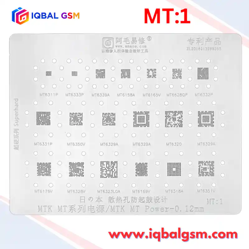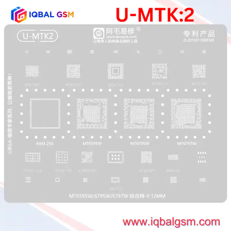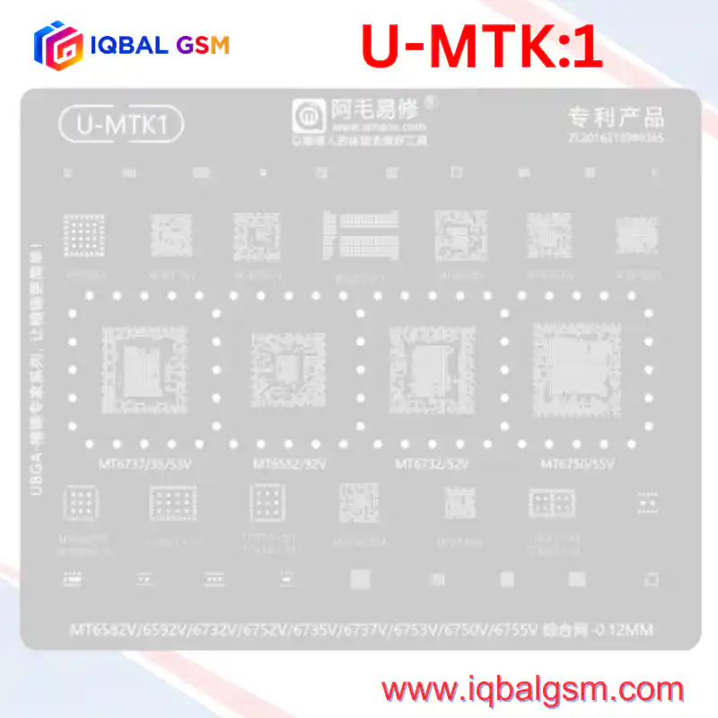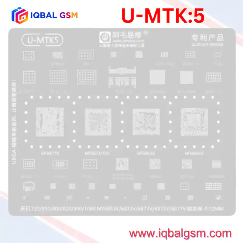

MU-2
As low as
Rs 700.00
Worldwide shipping · Cash on Delivery
Product Details
================================================================================
1. CHIP-LEVEL HARDWARE ARCHITECTURE & SILICON TOPOLOGY (MTK MU:2)
================================================================================
The AMAOE MU:2 stencil is dedicated to MediaTek's highest-volume legacy 3G and early 64-bit
4G LTE smartphone processors, which form the bedrock of entry-level and commercial device repairs:
A. APPLICATION PROCESSORS & SUBSTRATE ARCHITECTURES:
- MT6735 / MT6735V (64-Bit WorldMode LTE):
* Fabrication & Package: 28nm HPM process node, fine-pitch BGA footprint.
* Core Architecture: 4x ARM Cortex-A53 cores running up to 1.3 GHz - 1.5 GHz paired with
ARM Mali-T720 GPU and integrated baseband modem (supporting CDMA2000, TD-SCDMA, WCDMA, and LTE).
* Common Failure Mode: High operating temperatures in budget plastic-chassis phones cause solder
fatigue and micro-cracks along the central VCORE buck inductor power balls and peripheral ground pins.
Symptoms: Constant reboot loops on the carrier/vendor logo, spontaneous restarts under video playback,
or complete failure to boot (drawing a fixed 30 mA - 50 mA on DC bench supply). Reballing MT6735
with the MU:2 stencil permanently eliminates internal pad oxidation and joint fractures.
- MT6582 / MT6582V (32-Bit Quad-Core 3G):
* 28nm low-power SoC featuring 4x Cortex-A7 cores @ 1.3 GHz. Paired with discrete eMMC storage
and discrete MT6323GA PMIC.
* Physical stress vulnerability: Drop impacts frequently crack the corner anchor balls, disconnecting
the TX/RX baseband lines or the 26 MHz master clock input.
- MT6580 / MT6580A (Universal Entry Workhorse):
* Quad-core Cortex-A7 @ 1.3 GHz powering millions of budget Android Go and entry-level smartphones.
* Often paired with MT6350V or MT6323GA PMIC.
B. POWER & BOOT SEQUENCE HANDSHAKE:
- Primary Power Inputs:
* VPROC (CPU Core Rail): 0.7V - 1.25V dynamic buck voltage.
* VCORE (System Logic): 1.05V fixed buck voltage.
* VIO18 (Digital I/O): 1.8V reference rail supplied by PMIC.
* VEMC / VMCH: 3.0V / 3.3V power rails to external eMMC storage.
- Diagnostic Rule: If VIO18 (1.8V) and VCORE (1.05V) are present on the motherboard buck coils but
the phone hangs at 40 mA current draw, MT6735/MT6582 is in an unseated or cold-joint state, failing
to release WATCHDOG / RESET handshakes.
================================================================================
2. SOLDER PASTE SELECTION & THERMAL PARAMETERS
================================================================================
- Stencil Thickness: Exactly 0.12 mm laser-cut hardened Japanese stainless steel.
- Solder Paste Alloy:
* Sn63/Pb37 (63% Tin / 37% Lead) Eutectic Alloy: Melting Point 183°C.
* Particle Mesh Size: Type 4 (20 - 38 microns) or Type 5 (15 - 25 microns) mesh.
* Flux Formulation: No-Clean / Rosin Mildly Activated (RMA) high-viscosity tacky flux.
- Temperature Guidelines:
* Stencil Ball Reflow: 300°C - 320°C hot air, 25% - 30% airflow.
* Motherboard Desoldering: 345°C - 355°C (with bottom preheater at 140°C - 150°C).
* Motherboard Installation / Reflow: 335°C - 350°C until self-alignment occurs.
================================================================================
3. CHIP-LEVEL REWORK & REBALLING WORKFLOW
================================================================================
STEP 1: IC EXTRACTION
1. Mount the motherboard in a dedicated PCB repair fixture. Protect surrounding plastic FPC
connectors, SIM card slots, and camera sockets with aluminum heat-deflector tape.
2. Bottom Pre-Heat: Apply 140°C - 150°C across the board underside.
3. Apply tacky flux around the perimeter of the target SoC (e.g., MT6735V or MT6582).
4. Using an 8 mm circular nozzle on the hot-air station, set temperature to 350°C (airflow 45%).
5. Heat in smooth, continuous rectangular motions 1.5 cm above the chip for 25-35 seconds.
6. Verify solder liquefaction by nudging an adjacent surface-mount capacitor. Lift the chip straight
up using precision vacuum tweezers or ultra-fine curved tweezers (#5). Avoid any lateral prying.
STEP 2: PAD RESURFACING & EPOXY REMOVAL
1. Lower hot air to 250°C. Apply moderate RMA flux and gently scrape softened underfill glue from the
PCB pads and IC package margins using a non-scratch copper scraper blade.
2. Tin the footprint pads with 183°C leaded solder using a 330°C micro-soldering iron (C210-K knife tip).
3. Lay high-purity copper desoldering wick across the pads and glide the flat iron face across the
wick without applying downward pressure.
4. Level the IC base pads until smooth and planar. Clean with 99.9% IPA until mirror-clean.
STEP 3: REBALLING WITH THE AMAOE MU:2 STENCIL
1. Seat the cleaned IC into a magnetic reballing fixture.
2. Overlay the corresponding aperture on the MU:2 stencil:
- For MT6735 / MT6735V, align with "MT6735".
- For MT6582 / MT6582V, align with "MT6582".
- For MT6580 / MT6580A, align with "MT6580A".
- For MT6589, align with "MT6589".
- For Helio P10, align with "MT6755".
3. Verify that the circular anti-bulging expansion holes surround the chip perimeter to prevent
stencil warping under heat.
4. Spread Sn63/Pb37 paste into the apertures at a 45° angle with a flexible steel spatula. Wipe the
surface 100% clean of excess solder beads.
5. Hold the stencil down firmly at the margins with bent-tip titanium tweezers.
6. Direct hot air at 310°C - 325°C (airflow 25% - 30%) 3 cm above the stencil, moving inward.
Observe the paste coalesce into uniform spherical balls.
7. Allow 8-10 seconds to cool and solidify before lifting the stencil vertically.
8. Apply a drop of liquid flux and pass hot air for 3 seconds at 300°C for final spherical centering.
STEP 4: MOTHERBOARD INSTALLATION
1. Spread a micro-thin layer of tacky flux across the PCB pads (shiny, not flooded).
2. Align the IC with the PCB silkscreen corner brackets (verify Pin 1 dot orientation).
3. Reflow with hot air at 340°C - 350°C (airflow 40%). When the solder melts, surface tension will pull
the IC into exact alignment. Give a gentle 0.1 mm tweezer nudge: the chip must snap back immediately.
================================================================================
4. ELECTRICAL DIAGNOSTICS & FAULT MATRIX
================================================================================
1. Diode-Mode Impedance Verification (Unpowered board, Red probe to GND, Black probe to test point):
- VPROC / VCORE Buck Coils (MT6328 / MT6323) : 0.035 V - 0.110 V (Normal low-impedance buck loop).
- VIO18 (1.8V System I/O Rail) : 0.380 V - 0.490 V (Short indicates PMIC/SoC bridge).
- VBAT / VSYS (Primary Battery Rail) : 0.420 V - 0.540 V.
- eMMC VCC / VCCQ Storage Supplies : 0.410 V - 0.520 V.
2. DC Power Supply Boot-Up Analysis (4.0V DC Input on VBAT):
- 0.000 A Standby: Normal prior to pressing Power button.
- 15 mA - 80 mA Leakage (Pre-Power): Blown high-side buck MOSFET inside PMIC or shorted protection diode.
- Press Power -> Fixed 30 mA - 50 mA: PMIC has powered on, but 26 MHz master clock is missing,
or RESETB line is held low by the CPU.
- Press Power -> Cycles 70 mA -> 130 mA -> Drops to 0 mA: CPU has initialized; external eMMC storage
is unseated, unpowered, or missing firmware communication. Reball the eMMC BGA-221/BGA-153 chip.
- Normal Boot Progression: Steps steadily from 80 mA -> 240 mA -> 550 mA -> 1.0 A+ into Android OS.