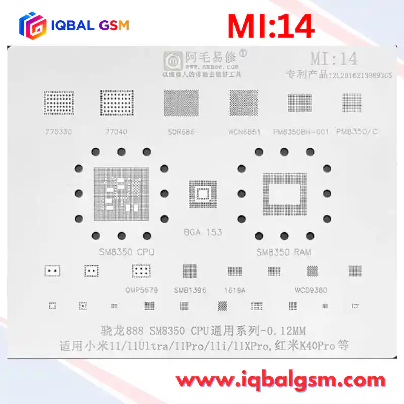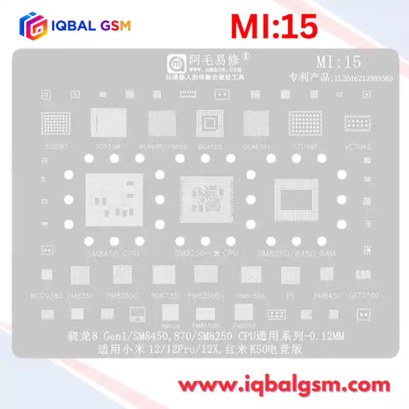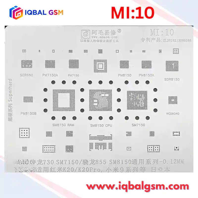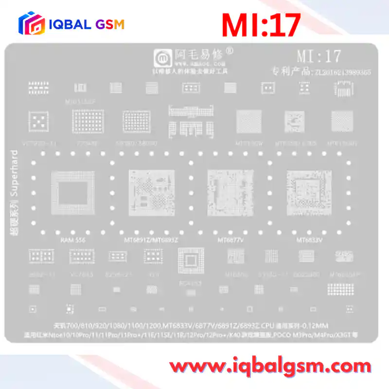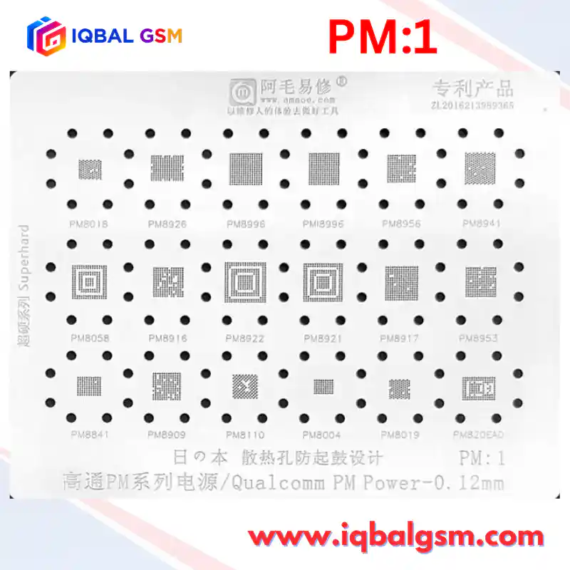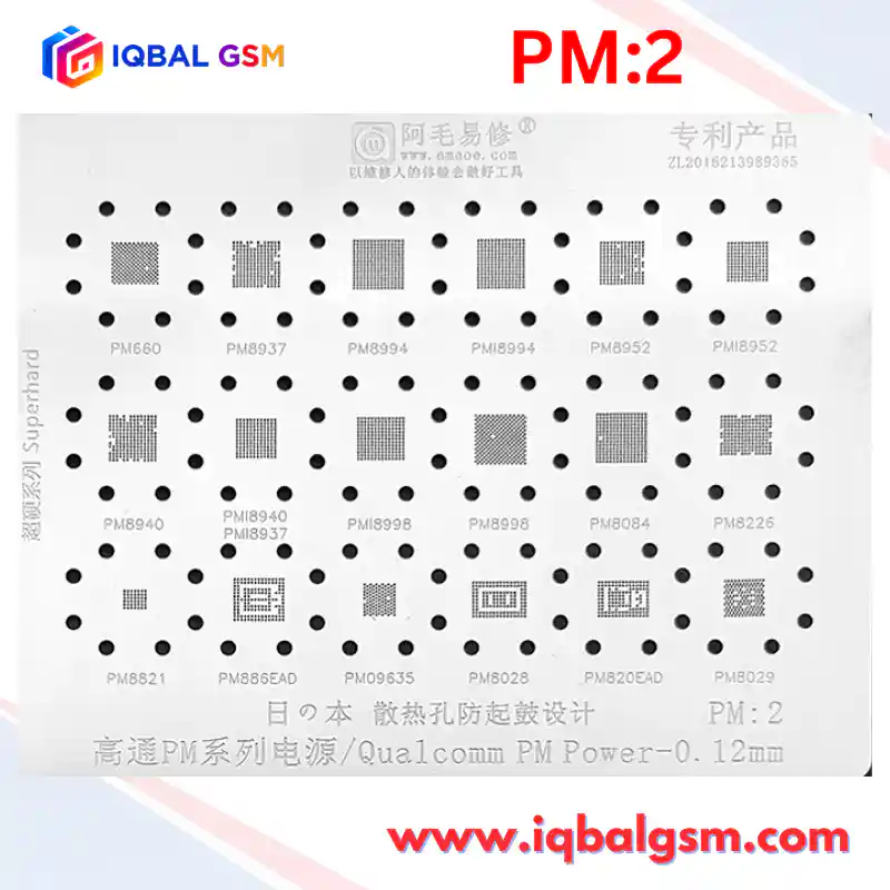

U-QSD7
As low as
Rs 700.00
Worldwide shipping · Cash on Delivery
Product Details
================================================================================
AMAOE U-QSD7 TECHNICAL REWORK, SILICON POWER ARCHITECTURE & DIAGNOSTIC GUIDE
================================================================================
1. SILICON POWER DOMAINS & ARCHITECTURAL OVERVIEW:
The U-QSD7 stencil services the modern mid-range Qualcomm 5G ecosystem, primarily centered on the SM7250 (Snapdragon 765G with integrated X52 modem) and SM7225/SM6375 (Snapdragon 750G / 695) platforms.
A. Multi-PMIC Power Management Architecture:
- Primary PMIC (PM7250 / PM6350):
* Converts main battery supply (VBAT) into the global system switched rail (VPH_PWR, 3.4V - 4.4V).
* Synchronous Buck Regulators generate core digital logic rails:
- VDD_CORE / VDD_APC0 (Silver cluster): 0.60V - 0.95V dynamic voltage scaling (DVS).
- VDD_APC1 (Gold/Prime cluster): 0.65V - 1.05V high-performance rails.
- VDD_MODEM: Dedicated 0.55V - 0.85V rail powering the internal Snapdragon X52 5G DSP engine.
- Secondary PMIC (PM7250B / PM6150L):
* Generates memory rails: VDD_MEM / VDDQ (0.6V / 1.1V for LPDDR4X).
* Supplies RF Transceiver rails (SDR865 / SDR735): 1.8V analog, 1.2V PLL, 0.9V digital.
* Hosts battery fast-charging controllers and display AMOLED bias rails (+4.6V / -4.0V).
B. Master Clock Synchronization & Power-On Sequence:
- 38.4 MHz Main Master Crystal (BB_CLK): Powers baseband PLLs inside the SoC and PMIC.
- 32.768 kHz Sleep Crystal (RTC): Keeps sleep clock and base counter active.
- Cold Boot Milestones:
1. VPH_PWR reaches stable 3.8V.
2. PM7250 activates LDO standby lines: VREG_L5A_1P8 (1.8V) and VREG_L3A_1P0 (1.0V).
3. Power Key pulled LOW pulls PMIC pin to ground -> PMIC starts buck power-up sequencing.
4. CPU releases reset and asserts PS_HOLD (1.8V) to latch PMIC output power registers.
5. CPU queries UFS storage via high-speed differential pairs (UFS_TX / UFS_RX) to load Primary Boot Loader (PBL) into internal SRAM.
--------------------------------------------------------------------------------
2. THERMAL GRADIENT, SOLDERING ALLOY STRATEGY & STENCIL MANAGEMENT:
- Solder Alloy Selection:
* CPU (SM7250 / SM7225 / SM6375) and Core PMICs: Sn63/Pb37 eutectic paste (Melting point: 183°C).
* BGA254 UFS Memory: Sn63/Pb37 (183°C) ensures structural rigidity during subsequent board reflows.
* Low-Temperature Solder Paste Warning: Sn42/Bi58 (138°C) is STRICTLY PROHIBITED for CPUs, PMICs, and 5G RF PAs. The high peak currents drawn during 5G uplink (exceeding 3.5A through VDD_APC buck inductors) cause thermal fatigue, micro-cracks, and electromigration in bismuth alloys, leading to device crashes under gaming or network loads.
- Solder Paste Preparation:
* Press paste onto lint-free wipes until excess flux oil is extracted, producing a dry, workable clay consistency. This prevents solder ball bridging and boiling ejection through the 0.12mm apertures.
- Thermal Profiling for 0.12mm SUS304 Stencil:
* Preheating: 150°C - 170°C for 30 seconds across the underside of the PCB.
* Hot Air Gun: 280°C - 300°C (Airflow: 25% - 30%) with a wide round nozzle. Sweep in an oval pattern around the edges first, moving to the center as the solder powder melts into bright spheres.
* Cooling: Hold stencil static for 5 seconds before lifting to prevent hot deformation of the balls.
--------------------------------------------------------------------------------
3. STEP-BY-STEP HOT AIR DESOLDERING, CLEANING & MOUNTING WORKFLOW:
STEP 1: Resin Underfill Removal
- SM7250 / SM7225 boards are sealed with rigid black or clear epoxy resin.
- Mount PCB into an anti-static alloy motherboard fixture.
- Set hot air station to 240°C - 250°C (Airflow: 35%).
- Using a 007-style micro-hook knife, gently scrape away perimeter underfill around the processor and memory. Avoid gouging the solder mask to prevent exposing ground copper.
STEP 2: Component Extraction
- Protect surrounding plastic connectors and secondary PMICs with thermal insulation tape and copper foil.
- Apply NC-559-ASM tacky flux around the chip boundary.
- Set hot air gun to 350°C - 365°C (Airflow: 50% - 60%).
- Hover 2 cm above the die in continuous rectangular sweeps.
- After 35-50 seconds, test corner buoyancy with ultra-fine tweezers. Once molten surface tension is confirmed, lift the SoC vertically. Never pull with mechanical force.
STEP 3: Motherboard & Chip Pad Leveling
- PCB Cleanup: Apply rosin flux and clean the PCB pads using a JBC C245-784 or T12-K knife tip at 340°C combined with 2.5mm copper desoldering wick (Goot Wick). Keep the iron tip flat to prevent scratching pads.
- Clean thoroughly with anhydrous 99.9% isopropyl alcohol until all flux residue is dissolved. Inspect under stereomicroscope for missing corner dummy pads or bridged lines.
- Chip Cleanup: Place the processor into a reballing jig. Apply flux and level bottom solder balls flat using the knife tip at 320°C. Clean clean with IPA.
STEP 4: Precision Reballing via U-QSD7
- Align the processor into the dedicated U-QSD7 aperture.
- Clamp stencil securely. Spread conditioned 183°C solder paste flat across the holes with a flexible 45-degree scraper. Wipe excess surface paste clean.
- Heat at 290°C - 310°C (Airflow: 25%) until all balls form uniform, shiny spheres.
- Allow cooling, apply a drop of liquid alcohol to the rear side, and push the IC out cleanly. Reheat the bare chip lightly with flux at 300°C to re-round the balls.
STEP 5: Alignment & Final Board Reflow
- Smear a microscopic, ultra-thin sheen of tacky flux onto the motherboard landing pads.
- Align the IC with the printed corner silkscreen markers.
- Heat with hot air at 330°C - 345°C (Airflow: 40%).
- When the solder reaches melting point, the chip will automatically center itself via surface tension. Give the IC a microscopic lateral nudge with tweezers; it must rebound immediately to prove 100% molten ball collapse.
--------------------------------------------------------------------------------
4. DIAGNOSTIC MATRIX & COLD DIODE-MODE / DC POWER SUPPLY FAULT SIGNATURES:
A. DC Power Supply (4.0V Injection into VPH_PWR / VBAT) Current Diagnostics:
┌──────────────────────┬────────────────────────────────┬────────────────────────────────────────────────────────┐
│ Current Reading │ Operational Stage │ Root Cause & Component Target │
├──────────────────────┼────────────────────────────────┼────────────────────────────────────────────────────────┤
│ 0.000A (Static) │ No reaction on Power Button │ Open PWR_KEY line; defective PM7250; shorted internal │
│ │ │ LDO clamping the PMIC; dead 38.4 MHz crystal. │
├──────────────────────┼────────────────────────────────┼────────────────────────────────────────────────────────┤
│ 2.5A - 5.0A (OCP) │ Immediate current surge/trip │ Short on VPH_PWR line; high-side MOSFET failure in │
│ │ (Full VBAT Short) │ PM7250 / PM6350; shorted decoupling capacitor. │
├──────────────────────┼────────────────────────────────┼────────────────────────────────────────────────────────┤
│ 0.025A - 0.060A │ Fixed current upon power press │ Missing 38.4 MHz baseband clock; PM7250 VREG_L5A_1P8 │
│ (Freeze) │ │ rail shorted; CPU core logic buck missing. │
├──────────────────────┼────────────────────────────────┼────────────────────────────────────────────────────────┤
│ 0.070A - 0.120A │ Constant steady draw (Qualcomm │ Qualcomm Emergency Download (EDL 9008) mode. Missing │
│ (Freeze) │ EDL State) │ UFS storage power (VCC 2.85V / VCCQ 1.2V), cold joint │
│ │ │ on UFS BGA254, or corrupt UFS boot partition. │
├──────────────────────┼────────────────────────────────┼────────────────────────────────────────────────────────┤
│ 0.080A -> 0.250A -> │ Infinite Restart Bootloop │ Missing PS_HOLD latch from CPU; defective buck coil on │
│ 0.000A │ (Cycles every 2-3 seconds) │ VDD_APC0/1; cold solder joint on secondary PMIC. │
├──────────────────────┼────────────────────────────────┼────────────────────────────────────────────────────────┤
│ 0.180A - 0.350A │ AP Initialization Hang │ CPU cold joint on LPDDR4X memory interface; UFS data │
│ (Freeze) │ │ line open; damaged Adreno 620 GPU core power rail. │
└──────────────────────┴────────────────────────────────┴────────────────────────────────────────────────────────┘
B. Cold Diode-Mode Ground Reference Values (Red Probe on Ground, Black on Test Point):
- PM7250 / PM6350 Primary Buck Coils:
* VDD_APC0 (Silver Cores): 0.120V - 0.190V (Extremely low resistance is normal; <0.020V indicates core short)
* VDD_APC1 (Gold/Prime Cores): 0.110V - 0.180V
* VDD_CORE (Digital Logic): 0.190V - 0.280V
* VDD_MODEM (Integrated X52 Baseband): 0.160V - 0.240V
* VPH_PWR Primary Power Bus: 0.380V - 0.460V
* VREG_L5A_1P8 (System 1.8V IO Rail): 0.460V - 0.540V
- BGA254 UFS Memory Test Points:
* UFS_VCC (2.85V Core Flash): 0.480V - 0.580V
* UFS_VCCQ (1.2V Logic): 0.380V - 0.450V
* UFS_VCCQ2 (1.8V IO): 0.490V - 0.560V
* UFS_TX_P / UFS_TX_M (Data Transmit Pairs): 0.420V - 0.480V (Must match within +/- 0.005V)
* UFS_RX_P / UFS_RX_M (Data Receive Pairs): 0.420V - 0.480V (Must match within +/- 0.005V)
- SDR865 / SDR735 RF Transceivers:
* VREG_SDR_1P8: 0.450V - 0.520V
* VREG_SDR_0P9: 0.310V - 0.390V
* Baseband I/Q Differential Pairs: 0.500V - 0.560V
================================================================================