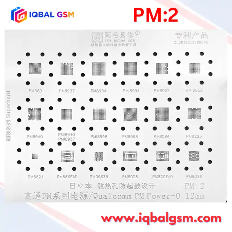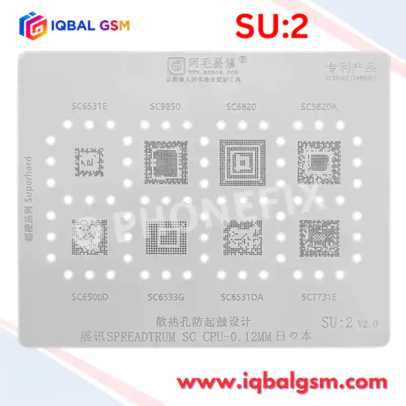

PM-1
As low as
Rs 700.00
Worldwide shipping · Cash on Delivery
Product Details
QUALCOMM PM POWER SYSTEM ARCHITECTURE & POWER TOPOLOGY
1. MASTER PMIC VS. SUB-PMIC DUAL-RAIL POWER ARCHITECTURE
- In modern Qualcomm Snapdragon designs, power distribution is split across two coordinated ICs:
* Master PMIC (e.g., PM8996, PM8953, PM8956): Houses the Always-On LDOs, real-time clock (RTC), power-key debounce logic, system reset supervisory circuits, sleep clock generator (32.768 kHz crystal oscillator driver), crystal oscillator buffer (CXO 19.2 MHz / 38.4 MHz), multi-channel high-efficiency SMPS buck regulators (VDD_CORE, VDD_APC0, VDD_APC1, VDD_MEM, VDD_IO), and SPMI (System Power Management Interface) slave bus interface.
* Secondary / Sub-PMIC (e.g., PMI8996): Integrates the high-efficiency switching battery charger (up to 3.0A Quick Charge 3.0), USB Type-C / Micro-USB CC-pin detection, OTG boost converter (5V @ 1.5A), WLED backlight driver (up to 29V boost array), haptic motor driver, and auxiliary high-current buck converters (VDD_APC_CORE auxiliary rails).
- Inter-IC Control & Synchronization:
* The Master and Sub-PMIC communicate with the Application Processor (AP) via the bidirectional Qualcomm SPMI bus (SPMI_CLK and SPMI_DATA), operating at 19.2 MHz. A defect or cold solder joint on either SPMI line locks the entire power distribution network, halting voltage sequencing.
2. POWER-ON SEQUENCING & BOOTSTRAP STAGES (MSM8953 / PM8953 / PM8996 BENCHMARK)
- Stage 1: VBAT / VPH_PWR Generation
* Direct battery connection (VBAT = 3.7V - 4.2V) enters the charging circuit. The buck-boost stage creates the main system rail: VPH_PWR (3.6V - 4.2V).
* VPH_PWR branches across every primary buck input terminal on the PMIC.
- Stage 2: Always-On Rails & Oscillator Initialization
* PMIC generates LDO1 / LDO2 standby rails: VDD_AO_1P8 (1.8V) and VDD_AO_0P8 (0.8V).
* Power key pull-up voltage (PWR_KEY_N = 1.8V) is asserted.
* 32.768 kHz RTC Sleep Clock begins oscillating and stabilizes.
- Stage 3: Power Key Trigger (PWR_KEY_N Pulled Low)
* When PWR_KEY_N is held low (<0.5V) for >100ms, the PMIC internal State Machine triggers cold boot.
* PMIC enables the 19.2 MHz Master CXO crystal oscillator buffer and asserts CXO_EN.
- Stage 4: Progressive Multi-Buck Stage Activation
* Buck 1 (VDD_DIG_0P95 / 0.95V): AP digital baseband core rail.
* Buck 2 & Buck 3 (VDD_APC0 / VDD_APC1 / 0.85V - 1.15V dynamic VID): CPU cluster cores.
* Buck 4 (VDD_MEM / 1.2V LPDDR3 or 1.1V LPDDR4): RAM array voltage.
* Buck 5 (VDD_IO / 1.8V): System interface logic voltage.
- Stage 5: LDO Cascade & System Power Good (PS_HOLD)
* After all bucks reach steady-state regulation within +/-2% tolerance, peripheral LDOs fire sequentially (UFS/eMMC VCC 3.0V, VCCQ 1.8V, Sensor rails 1.8V/2.8V).
* Master PMIC asserts RESET_N (1.8V) to release CPU from reset.
* CPU executes PBL (Primary Bootloader) from internal ROM. If memory initialization passes, CPU pulls PS_HOLD high (1.8V) back to the PMIC within 500ms.
* CRITICAL: If PS_HOLD fails to latch high within 500ms, the PMIC cuts all buck rails and restarts the cycle (bootloop or immediate shutoff).
STEP-BY-STEP HOT AIR REWORK & REBALLING METHODOLOGY
1. CHIP DESOLDERING & PCB SITE PREPARATION
- Heat Sink / Shield Removal:
* Apply mechanical Kapton tape (polyimide) combined with 0.1mm copper foil over adjacent baseband processors, UFS/eMMC flash storage, and CPU/RAM package to prevent secondary ball shorting.
- Hot Air Gun Parameters (Pre-Heating & Extraction):
* Nozzle: 6mm - 8mm angled smooth-bore nozzle.
* Station Settings: Temperature: 345°C - 355°C | Airflow: 50% - 55% (Quick 861DW benchmark).
* Technique: Apply synthetic RMA-218 or NC-559-ASM no-clean paste flux sparingly around the chip perimeter. Pre-heat the entire PCB area within a 3cm radius for 20-30 seconds using spiral circular motions. Concentrate heat uniformly over the PMIC package.
* Removal: Touch the edge of the PMIC gently with curved fine tweezers. Once all solder joints liquefy (visual surface tension collapse), lift the IC vertically at a 90° angle. NEVER apply upward leverage before total reflow, or copper BGA pads will tear from the PCB substrate.
- Motherboard BGA Site Cleaning:
* Apply leaded rosin flux and use a copper desoldering wick (2.0mm width) under a soldering iron chisel tip (T12-D24 or C210-020) at 320°C - 340°C.
* Flatten all residual solder bumps until pads are perfectly planar.
* Clean thoroughly with pure anhydrous isopropyl alcohol (IPA) and an ESD bristle brush. Inspect under stereo microscope for pad oxidation, pad bridging, or damaged solder mask.
2. PRECISION REBALLING WITH AMAOE PM:1 STENCIL
- Solder Alloy Selection:
* For Qualcomm PMICs, use Leaded Low-to-Medium Temperature Solder Paste: Sn63/Pb37 (Melting Point: 183°C).
* DO NOT use 138°C Bi-Sn low-temp alloy on primary PMICs: under heavy multi-core processing or Fast Charging (QC 3.0 / QC 4.0), PMICs can reach junction temperatures of 85°C - 105°C, causing 138°C solder balls to soften, undergo electromigration, crack, or short.
- Stencil Mounting & Alignment:
* Place the cleaned PMIC into the corresponding engraved aperture of the AMAOE PM:1 stencil.
* Align all BGA pad openings under 10x-20x magnification. Ensure the stencil rests 100% flush without curvature.
- Paste Application & Drying:
* Squeeze a small dab of Sn63/Pb37 solder paste onto dust-free lens paper and press firmly with a spatula to absorb excess flux solvent until the paste achieves a matte, thick putty-like consistency.
* Spread paste into the stencil apertures using a semi-rigid stainless steel squeegee held at a 45° angle, filling all holes uniformly. Wipe clean with lint-free wipes in a single diagonal stroke.
- Thermal Forming of Solder Spheres:
* Station Settings: Temperature: 280°C - 300°C | Airflow: 25% - 30% (Low airflow to avoid ball popping/blowaway).
* Keep nozzle at a distance of 3cm - 4cm, heating the stencil perimeter first to prevent thermal warping of the steel plate.
* Move nozzle over the aperture array in slow continuous circles. Observe the paste turn to liquid metal spheres and latch onto the gold-nickel pads.
* Allow 10 seconds of cooling until solder solidifies, then gently release the chip from the stencil underside using ESD tweezers.
- Post-Reball Secondary Reflow:
* Apply a microscopic droplet of liquid or light gel flux over the reballed IC.
* Reflow at 280°C hot air for 3-5 seconds. Surface tension will pull every solder sphere into a perfectly uniform, gleaming spherical shape.
3. RE-SOLDERING & CHIP PLACEMENT
- Apply a micro-thin, uniform layer of high-tack flux across the motherboard BGA pad array.
- Align the Pin 1 orientation index (laser dot / marker on PMIC corner) precisely with the motherboard silkscreen corner bracket.
- Hot Air Soldering Parameters:
* Temperature: 330°C - 340°C | Airflow: 40% - 45%.
* Heat perpendicularly from 2cm height in uniform circular motions.
* Watch the chip sink slightly as the 183°C solder balls reflow. Tap the corner of the silicon die gently with micro-tweezers (<0.2mm lateral displacement); if properly soldered, the chip will instantly spring back into place via the self-centering surface tension of the molten solder balls.
- Cool naturally for 2 minutes before powering up.
COLD DIODE-MODE & DC SUPPLY FAULT DIAGNOSIS MATRIX
1. BENCH DC POWER SUPPLY CURRENT-CONSUMPTION PROFILES (4.0V VPH_PWR / VBAT INPUT)
- Profile A: Direct Short Circuit (0.000A -> Pegs 2.0A - 5.0A OCP Shutdown upon connection)
* Defect: Primary VPH_PWR rail or VBAT input filter shorted to ground.
* Root Cause: Shorted high-side MOSFET inside PMIC, or shorted external bypass capacitor on VPH_PWR (e.g., 22uF/10V ceramic capacitors near the main inductor).
* Action: Connect DC supply at 1.2V / 3A with thermal camera. Identify glowing component. If PMIC glows instantly at 0V, replace PMIC.
- Profile B: Zero Current Draw on Power Key Press (0.000A Static)
* Defect: Power Key circuit open or PMIC standby logic completely dead.
* Root Cause: No 1.8V pull-up on PWR_KEY_N line; dead 32.768 kHz RTC crystal; missing VDD_AO standby rail; cracked solder ball under PM8953/PM8996 VBAT sense pins.
- Profile C: Micro-Current Freeze (Pulses 0.020A - 0.045A and holds indefinitely)
* Defect: PMIC wakes up, but secondary buck regulators fail to start or 19.2 MHz clock fails.
* Root Cause: Defective 19.2 MHz CXO crystal or missing CXO_EN; short circuit on VDD_DIG_0P95 or VDD_APC core voltage rails.
- Profile D: Medium-Current Bootloop (Hunts 0.080A -> 0.180A -> Drops to 0.000A -> Loops)
* Defect: Missing PS_HOLD handshake from CPU.
* Root Cause: PMIC releases RESET_N, but AP cannot read PBL from UFS/eMMC due to memory power failure (VDD_MEM / VCCQ missing) or corrupt bootloader.
- Profile E: High-Current Boot Freeze (Jumps directly to 0.450A - 0.900A without boot cycling)
* Defect: Short circuit or heavy leak on secondary LDO rails (Display 2.8V, Camera 1.2V/2.8V, Baseband RF 1.8V).
2. COLD DIODE-MODE IMPEDANCE MATRIX (RED PROBE TO GND, BLACK PROBE TO TARGET PIN/CAPACITOR)
- Benchmark values measured on typical PM8953 / PM8996 power nodes:
* VPH_PWR Input Rail : 0.380V - 0.460V (If <0.100V: Primary rail shorted)
* VDD_APC0 Core Buck (L4000) : 0.080V - 0.150V (Low baseline resistance is normal for AP core)
* VDD_APC1 Core Buck (L4001) : 0.080V - 0.150V (If 0.000V: Direct silicon core short)
* VDD_MEM LPDDR Rail (L4002) : 0.280V - 0.340V (If <0.120V: RAM die compromised)
* VDD_IO System Rail (L4003) : 0.360V - 0.420V (If <0.200V: Digital peripheral bus shorted)
* VREG_L6_1P8 (SPMI Bus Pull-up) : 0.420V - 0.480V (If open-circuit OL: SPMI interface disconnected)
* PWR_KEY_N Pin : 0.580V - 0.650V (If OL: Traced trace break to PMIC ball)
* PS_HOLD Line : 0.450V - 0.520V (If 0.000V: AP line shorted or PMIC internal diode blown)