
PM-2
As low as
Rs 700.00
Worldwide shipping · Cash on Delivery
Product Details
QUALCOMM PM POWER SYSTEM ARCHITECTURE & POWER TOPOLOGY
1. DUAL-CHIP POWER ARCHITECTURE: MASTER PMIC & SUB-PMIC COOPERATION
- Snapdragon platforms represented on the AMAOE PM:2 stencil (e.g., SDM660 + PM660/PM660L, MSM8998 + PM8998/PMI8998, MSM8994 + PM8994/PMI8994) divide system power functions across two complementary ICs:
* Master PMIC (PM660, PM8998, PM8994, PM8937):
Contains the primary power-on state machine, real-time clock (RTC 32.768 kHz), primary crystal oscillator buffer (CXO 19.2 MHz / 38.4 MHz), power-key debounce circuit, hardware reset monitors, and multi-channel synchronous buck regulators supplying digital baseband core (VDD_DIG), CPU application cores (VDD_APC0 / VDD_APC1), system memory (VDD_MEM / LPDDR4 / LPDDR3), and system IO (VDD_1P8).
* Secondary / Sub-PMIC (PM660L, PMI8998, PMI8994, PMI8952, PMI8940, PMI8937):
Contains the switching battery charger (up to Quick Charge 4.0+), USB Type-C CC logic / BC1.2 charger detection, OTG 5V boost converter, WLED backlight driver (up to 29V output) or AMOLED dual-rail display bias (+/-4.6V VDD_DISP / VEE_DISP), torch/flash LED drivers, and supplemental high-current buck converters for GPU and secondary CPU clusters.
- SPMI Control Bus Architecture:
* Master and Sub-PMICs interface with the Application Processor (AP) via Qualcomm's 2-wire System Power Management Interface (SPMI_CLK and SPMI_DATA) running at 19.2 MHz. A cold solder joint, bridging, or trace open on either SPMI line locks the entire power state machine, preventing the AP from dynamically controlling voltages and causing an immediate shutdown or bootloop.
2. POWER-ON BOOT SEQUENCE & TIMING BENCHMARK (PM660 / PM8998 PLATFORM)
- Step 1: VPH_PWR Main System Rail Generation
* Upon connecting battery (VBAT 3.7V - 4.2V) or DC power supply / USB VBUS (5V - 9V), the Sub-PMIC (e.g., PMI8998/PM660L) buck-boost stage establishes the system master bus: VPH_PWR (3.6V - 4.2V).
* VPH_PWR distributes to all high-side MOSFET inputs of the buck converters inside both PMICs.
- Step 2: Always-On Standby Initialization & Sleep Clock
* Master PMIC generates Always-On LDO rails: VDD_AO_1P8 (1.8V) and VDD_AO_0P8 (0.8V).
* Power button pull-up line (PWR_KEY_N) is biased to 1.8V.
* The 32.768 kHz RTC Sleep Clock starts oscillating.
- Step 3: Hardware Power-On Trigger (PWR_KEY_N Assertion)
* Power button is pressed, grounding PWR_KEY_N (<0.5V) for >100ms.
* The Master PMIC internal Power-On State Machine awakens and asserts CXO_EN to turn on the 19.2 MHz Master System Crystal (XO).
- Step 4: Staged Multi-Buck Regulator Activation
* Buck 1 (VDD_DIG_0P85 - 0.95V): Primary digital logic core rail.
* Buck 2 (VDD_MEM_1P1 - 1.2V): LPDDR3 / LPDDR4 RAM core rail.
* Buck 3 & Buck 4 (VDD_APC0 & VDD_APC1): CPU Little and Big core dynamic VID rails (0.75V - 1.15V).
* Buck 5 (VDD_IO_1P8): Peripheral interface voltage.
- Step 5: Peripheral LDO Enablement & Reset Release
* Low-dropout regulators initialize sequentially: UFS/eMMC VCC (2.95V), UFS VCCQ (1.2V), eMMC VCCQ (1.8V), sensors, audio codec.
* Master PMIC releases the active-low hardware reset signal: RESET_N (1.8V) to the AP.
* AP reads Primary Bootloader (PBL) from internal ROM.
* Within 500ms of reset release, the AP must return PS_HOLD (1.8V) high to the Master PMIC.
* CRITICAL: If PS_HOLD remains low after 500ms, the PMIC assumes a processor crash, drops all buck rails to 0V, and either shuts down or attempts a hardware restart.
STEP-BY-STEP HOT AIR REWORK & REBALLING METHODOLOGY
1. CHIP REMOVAL & MOTHERBOARD BGA SITE PREPARATION
- Thermal Protection:
* Apply dual-layer thermal shielding: first a layer of polyimide (Kapton) tape, topped with 0.1mm adhesive copper foil over neighboring memory (UFS/eMMC), CPU, and RF transceiver ICs.
- Hot Air Gun Removal Parameters:
* Nozzle: 6mm - 8mm smooth circular nozzle.
* Air Station Parameters: Temperature: 345°C - 355°C | Airflow: 50% - 55% (Quick 861DW benchmark).
* Technique: Apply a small bead of synthetic RMA-218 or Amtech NC-559-ASM flux around the chip edges. Pre-heat the entire PCB quadrant in wide spiral circles for 25-30 seconds. Focus airflow uniformly over the top of the PMIC package.
* Extraction: Test the edge of the PMIC with fine curved tweezers. Once molten surface tension is confirmed, lift the chip vertically at 90°. Never pry or wrench an un-melted chip to avoid pulling BGA pads from the motherboard substrate.
- Motherboard Pad Planarization:
* Add leaded flux and use a 2.0mm copper desoldering braid under a soldering iron chisel tip (T12-D24 / C210-020) at 320°C - 340°C.
* Sweep lightly across the pad array until all residual solder mounds are removed and pads are completely flat.
* Clean thoroughly with pure anhydrous isopropyl alcohol (IPA) and inspect under a microscope for lifted pads, damaged solder mask, or bridging.
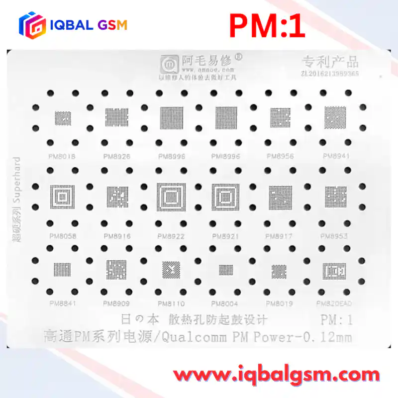
2. PRECISION REBALLING WITH AMAOE PM:2 STENCIL
- Solder Alloy Selection:
* Use Leaded Medium-Temperature Solder Paste: Sn63/Pb37 (Melting Point: 183°C).
* DO NOT use low-temperature bismuth alloy (138°C Sn42/Bi58) on Qualcomm primary or secondary PMICs. During Fast Charging (Quick Charge 3.0 / 4.0+) or sustained CPU/GPU workload, PM660 / PM8998 junction temperatures easily reach 85°C - 105°C. At these temperatures, 138°C solder undergoes severe thermal degradation, ball deformation, and solder bridging.
- Stencil Positioning:
* Seat the cleaned PMIC into its designated aperture on the AMAOE PM:2 plate.
* Verify under stereo magnification (10x-20x) that all BGA pads align squarely with the laser-cut apertures.
- Paste Application & Moisture Extraction:
* Place Sn63/Pb37 solder paste on lint-free paper and press firmly with a spatula to absorb excess flux oil. The paste should attain a firm, matte consistency.
* Scrape paste into the apertures with a stainless steel squeegee at a 45° angle. Ensure every aperture is 100% packed. Scrape the surface clean in one continuous diagonal pass.
- Solder Ball Formation:
* Air Station Parameters: Temperature: 280°C - 300°C | Airflow: 25% - 30% (Low airflow to avoid ball ejection).
* Hold the nozzle 3cm - 4cm above the stencil. Warm the perimeter first to prevent thermal plate distortion, then move in slow, circular motions over the apertures.
* Watch the solder melt and form gleaming spherical balls inside every aperture. Allow 10 seconds of cooling before gently separating the stencil from the chip.
- Secondary Ball Finishing:
* Dispense a micro-drop of liquid flux over the reballed IC.
* Reflow with hot air at 280°C for 3 seconds. Surface tension will perfect ball sphericity and eliminate any micro-burrs.
3. SOLDERING & SELF-CENTERING ALIGNMENT
- Apply a micro-thin layer of high-tack tacky flux across the motherboard BGA site.
- Align the Pin 1 index dot on the PMIC with the corresponding silkscreen corner mark on the PCB.
- Hot Air Soldering Parameters:
* Temperature: 330°C - 340°C | Airflow: 40% - 45%.
* Heat in smooth, wide circles around the chip perimeter, gradually closing inward.
* Once the solder reflows, the chip will settle slightly. Gently nudge one corner with fine tweezers (<0.2mm displacement); the IC will immediately bounce back into center position due to liquid solder surface tension.
- Allow 3 minutes of passive cooling before applying DC power.
COLD DIODE-MODE & DC SUPPLY BOOT DIAGNOSTIC MATRIX
1. BENCH DC POWER SUPPLY CURRENT SIGNATURES (4.0V VPH_PWR / VBAT HOOKUP)
- Fault Profile 1: Dead Short Circuit (0.000A -> Instant Over-Current Protection Trip @ 2.0A - 5.0A)
* Defect: Primary VPH_PWR bus or VBAT input shorted directly to ground.
* Root Cause: High-side MOSFET failure inside PMIC (PM660 / PM8998), or shorted 22uF/10V ceramic decoupling capacitor on VPH_PWR.
* Diagnostic Step: Inject 1.2V / 3A on VPH_PWR with a thermal camera. If the PMIC die lights up instantly at low voltage, the internal silicon bridge is blown.
- Fault Profile 2: Total Zero Current Draw on Power Key Press (0.000A Static)
* Defect: Power-on circuit non-responsive or standby supply missing.
* Root Cause: Open power button line (PWR_KEY_N missing 1.8V pull-up); dead 32.768 kHz RTC crystal; defective VDD_AO standby rail; cracked solder ball on PMIC VPH_PWR sense pins.
- Fault Profile 3: Micro-Current Freeze (0.025A - 0.050A Constant)
* Defect: Master PMIC wakes up, but secondary buck regulators or master clock fail.
* Root Cause: 19.2 MHz CXO crystal failed or CXO_EN missing; short circuit on VDD_DIG core buck (0.85V rail); open circuit on SPMI bus (SPMI_CLK / SPMI_DATA).
- Fault Profile 4: Bootlooping Pulse (0.070A -> 0.180A -> Drops to 0.000A -> Repeats)
* Defect: Missing PS_HOLD handshake from Application Processor.
* Root Cause: PMIC successfully generates all buck rails and releases RESET_N, but AP cannot read Primary Bootloader (PBL) due to missing RAM/UFS power (VDD_MEM / VCCQ) or corrupted boot partition.
- Fault Profile 5: Heavy Current Latch at Boot (Jumps straight to 0.500A - 1.200A without boot oscillation)
* Defect: Secondary peripheral LDO rail shorted to ground.
* Root Cause: Shorted display bias rail (+5V/-5V), shorted camera sensor rail (AVDD 2.8V), or shorted RF transceiver supply (1.8V RF).
2. COLD DIODE-MODE IMPEDANCE MATRIX (RED PROBE TO GND, BLACK PROBE TO TARGET TEST POINT/CAPACITOR)
- Baseline Diode-Mode Readings for PM660 / PM8998 / PM8937 Power Nodes:
* VPH_PWR Main Rail : 0.380V - 0.460V (If <0.100V: Primary system short)
* VDD_APC0 CPU Core Buck (Inductor): 0.070V - 0.130V (Low diode reading is normal for high-current AP core)
* VDD_APC1 CPU Core Buck (Inductor): 0.070V - 0.130V (If 0.000V: Silicon die shorted)
* VDD_MEM LPDDR Rail (Inductor) : 0.280V - 0.350V (If <0.120V: Memory array shorted)
* VDD_IO System Rail (Inductor) : 0.350V - 0.430V (If <0.200V: Digital interface rail shorted)
* VDD_DIG Baseband Core Buck : 0.250V - 0.320V (If <0.080V: Digital baseband core leak)
* SPMI_CLK / SPMI_DATA Bus Lines : 0.420V - 0.490V (If OL: Broken ball under PMIC/CPU; if 0.000V: Bus shorted)
* PWR_KEY_N Line : 0.580V - 0.680V (If OL: Broken circuit from flex connector to PMIC)
* PS_HOLD Test Point : 0.440V - 0.510V (If 0.000V: Shorted AP pin; if OL: Solder joint disconnect)