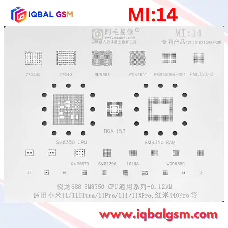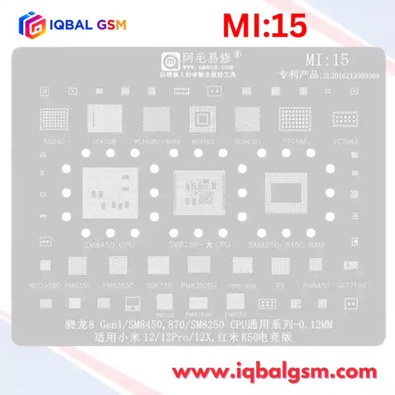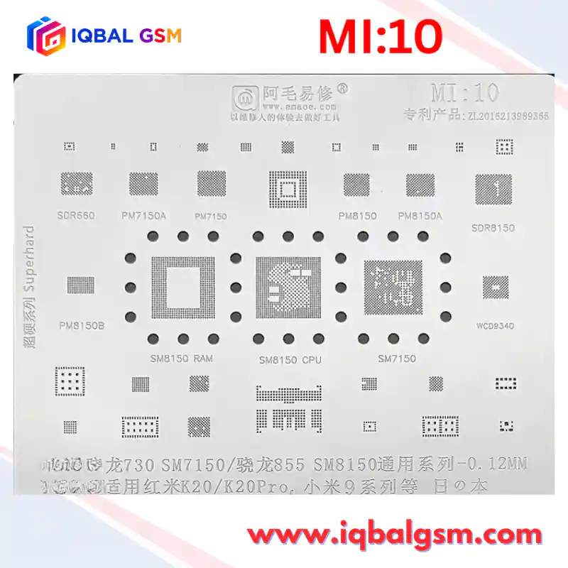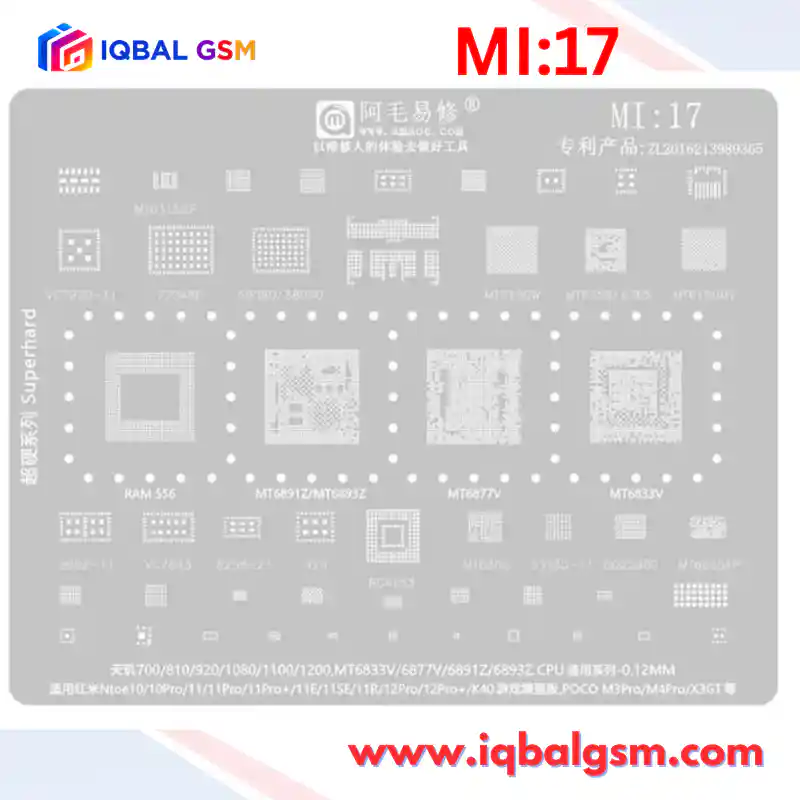

U-QSD6
As low as
Rs 700.00
Worldwide shipping · Cash on Delivery
Product Details
================================================================================
AMAOE U-QSD6 REWORK, SILICON POWER ARCHITECTURE & DIAGNOSTIC GUIDE
================================================================================
1. SILICON POWER DOMAINS & ARCHITECTURAL OVERVIEW:
The U-QSD6 stencil covers Qualcomm's high-tier 10nm (SDM845) and 7nm (SM8150) platforms, which feature complex multi-rail power distribution networks and stacked Package-on-Package (PoP) memory architecture.
A. Tri-PMIC Power Topology (SM8150 Architecture):
- PM8150 (Master PMIC):
* Generates VPH_PWR from battery/charger input (3.4V - 4.4V).
* Buck converters supply VDD_CORE (0.65V - 0.85V) for digital base logic and peripheral blocks.
* LDO network generates analog, PLL, and crystal reference supplies (e.g., VREG_L5A_1P8 for standard IO).
- PM8150A (Auxiliary Buck PMIC):
* Supplies high-current dynamic CPU rails:
- VDD_APC0 (Kryo 485 Silver cluster): 0.60V - 0.95V.
- VDD_APC1 (Kryo 485 Gold / Prime cluster): 0.65V - 1.10V (Peak drain > 10A during boost).
- PM8150B (Charger / Secondary Buck PMIC):
* Dedicated VDD_MODEM rail for Snapdragon X24 LTE / X50 external 5G baseband.
* Hosts battery fast-charging controllers and AMOLED panel bias supplies (+4.6V / -4.0V).
B. Master Clocks & Power-On Sequence:
- 38.4 MHz Main Master Crystal (BB_CLK): Connects to PM8150/SM8150 to synchronize internal PLLs.
- 32.768 kHz RTC Sleep Crystal: Sustains internal counter and low-power standby sleep cycles.
- Step-by-Step Power-Up Sequence:
1. VPH_PWR reaches nominal voltage (3.8V).
2. PM8150 internal reference engine stabilizes; always-on LDO rails activate (VREG_L5A_1P8 = 1.8V).
3. Power key pulled to GND triggers power-management state machine.
4. PM8150, PM8150A, and PM8150B enable sequential buck regulators in hardware-interlocked stages.
5. Master 38.4 MHz clock stabilizes -> PM8150 releases hardware RESET_N to the CPU.
6. CPU boots initial bootrom, sets PS_HOLD pin to 1.8V to lock PMIC power output registers.
7. CPU sends clock and commands across high-speed differential links to BGA254/BGA153 UFS storage.
--------------------------------------------------------------------------------
2. THERMAL GRADIENT, SOLDERING ALLOY STRATEGY & STENCIL MANAGEMENT:
- Solder Alloy Selection (Dual-Temperature PoP Strategy):
* Lower Layer (CPU to Motherboard): Sn63/Pb37 leaded solder paste (Melting point: 183°C).
* Upper Layer (RAM556 to CPU top): Sn63/Pb37 (183°C) or specialized medium-temperature Sn62/Pb36/Ag2 (179°C).
* Low-Temperature Solder Warning: Sn42/Bi58 (138°C) is STRICTLY PROHIBITED. High-performance gaming on Snapdragon 855 / 845 pushes die temperatures to 80°C - 85°C. Low-temp bismuth solder will undergo thermal fatigue, crystalline deformation, and electromigration, creating intermittent open circuits and catastrophic shutdowns under load.
- Solder Paste Viscosity Preparation:
* Knead the paste on absorbent lint-free paper until excess flux vehicle is drawn out, leaving a dry, putty-like paste. This eliminates bridging and prevents boiling flux splatter between adjacent fine-pitch apertures.
- Thermal Profiling for 0.12mm SUS304 Stencil:
* Preheating: 150°C - 170°C for 30 seconds on bottom preheater to minimize PCB warping.
* Stencil Heating: Hot air rework station set to 280°C - 300°C (Airflow: 25% - 30%). Use a sweeping circular motion from the periphery to the center until shiny, spherical solder balls form across all apertures.
--------------------------------------------------------------------------------
3. STEP-BY-STEP HOT AIR REWORK PROCEDURE FOR PACKAGE-ON-PACKAGE (PoP):
STEP 1: Adhesive Underfill Clearing
- Mount motherboard into a dedicated CNC aluminum clamp fixture.
- Set hot air station to 230°C - 240°C (Airflow: 35%).
- Using a fine 007 curved blade, carefully cut and remove black epoxy resin surrounding the CPU, RAM, and adjacent 0201 decoupling capacitors. Ensure no copper ground planes are exposed.
STEP 2: De-layering (RAM Removal First)
- Protect surrounding connectors and UFS memory with Kapton tape and copper heat sinks.
- Apply tacky rosin flux (NC-559-ASM) around the CPU/RAM stack.
- Hot air station: 340°C - 350°C (Airflow: 45%).
- Heat the top of the RAM evenly for 25 - 35 seconds. Insert an ultra-thin curved pry blade (0.05mm) between the RAM layer and the CPU top deck.
- As solder melts, gently lever the RAM off vertically. Do not apply downward force on the underlying CPU die.
STEP 3: Base CPU Removal
- Apply fresh flux around the bare CPU die.
- Increase hot air to 355°C - 365°C (Airflow: 55%).
- Heat the CPU evenly in broad rectangular passes. After 30 - 45 seconds, nudge the corner gently with micro-tweezers. When free float is confirmed, lift the CPU vertically.
STEP 4: Pad Dressing & Substrate Leveling
- Motherboard Cleanup: Apply flux and run a wide chisel tip (JBC C245-784 or T12-K) at 340°C with 2.5mm copper braid (Goot Wick). Remove all residual factory lead-free alloy (SAC305) until the pads are completely flat and level. Clean with 99.9% anhydrous IPA.
- CPU Dressing: Clean both the bottom BGA pads and top RAM seating pads using a knife tip at 320°C and fresh leaded solder. Remove residual underfill using a specialized brass wire brush at 220°C under the microscope.
STEP 5: Two-Stage Reballing via U-QSD6
- CPU Reballing: Fit the bottom of the SM8150 / SDM845 into the corresponding aperture. Spread prepared 183°C leaded paste, scrape flat, and heat at 290°C - 305°C (Airflow: 25%) until uniform balls form. Eject and reflow lightly with flux.
- RAM Reballing: Fit the RAM556 memory into the RAM aperture. Apply 183°C paste, heat evenly, and verify all 556 perimeter balls are of identical height under the microscope.
STEP 6: Sequential Installation (Base CPU -> Upper RAM)
- Lower Layer: Smear a microscopic layer of flux on the motherboard. Align the CPU with corner silkscreen guides. Heat at 335°C - 345°C (Airflow: 40%). Verify self-centering via a light horizontal nudge test. Allow board to cool completely.
- Upper Layer: Apply an ultra-thin sheen of tacky flux across the top deck of the installed CPU. Align the RAM556 chip carefully using perimeter alignment marks. Reflow at 320°C - 330°C (Airflow: 35%). When the RAM reaches molten phase, surface tension will snap it into alignment.
--------------------------------------------------------------------------------
4. DIAGNOSTIC MATRIX & COLD DIODE-MODE / DC POWER SUPPLY FAULT SIGNATURES:
A. DC Power Supply (4.0V Injection into VPH_PWR / VBAT) Current Diagnostics:
┌──────────────────────┬────────────────────────────────┬────────────────────────────────────────────────────────┐
│ Current Reading │ Operational Stage │ Suspected Root Cause & Troubleshooting Target │
├──────────────────────┼────────────────────────────────┼────────────────────────────────────────────────────────┤
│ 0.000A (Static) │ No reaction on Power Button │ Open PWR_KEY line; defective PM8150 / PM845; dead RTC │
│ │ │ 32.768 kHz or 38.4 MHz crystal; PMIC buck shorted. │
├──────────────────────┼────────────────────────────────┼────────────────────────────────────────────────────────┤
│ 2.5A - 5.0A (OCP) │ Immediate current surge/trip │ Main VPH_PWR line shorted to ground; breached high- │
│ │ (Full VBAT Short) │ side MOSFET in PM8150/PM8150A; shorted decoupling cap. │
├──────────────────────┼────────────────────────────────┼────────────────────────────────────────────────────────┤
│ 0.025A - 0.055A │ Fixed current upon power press │ Missing 38.4 MHz clock; VREG_L5A_1P8 rail shorted; │
│ (Freeze) │ │ CPU core logic buck missing; defective PM8150A. │
├──────────────────────┼────────────────────────────────┼────────────────────────────────────────────────────────┤
│ 0.070A - 0.120A │ Constant steady draw (Qualcomm │ Qualcomm Emergency Download (EDL 9008) mode. Missing │
│ (Freeze) │ EDL State) │ UFS storage power (VCC 2.85V / VCCQ 1.2V), cold joint │
│ │ │ on BGA153/BGA254, or corrupt UFS firmware partition. │
├──────────────────────┼────────────────────────────────┼────────────────────────────────────────────────────────┤
│ 0.080A -> 0.280A -> │ Infinite Restart Bootloop │ Missing PS_HOLD latch from CPU; unstable buck coil on │
│ 0.000A │ (Cycles every 2-3 seconds) │ VDD_APC0/1; cold solder joint on PM8150B or PM8150A. │
├──────────────────────┼────────────────────────────────┼────────────────────────────────────────────────────────┤
│ 0.220A - 0.450A │ AP Initialization Hang │ Upper RAM556 pseudo-soldering / bridge; missing VDDQ │
│ (Freeze) │ (DRAM Init Failure) │ (0.6V) or VDD2 (1.1V); damaged CPU memory controller. │
└──────────────────────┴────────────────────────────────┴────────────────────────────────────────────────────────┘
B. Cold Diode-Mode Ground Reference Values (Red Probe on Ground, Black on Test Point):
- PM8150 / PM8150A / PM845 Primary Buck Coils:
* VDD_APC0 (Silver Cores): 0.110V - 0.170V (Very low resistance is normal; <0.015V indicates silicone short)
* VDD_APC1 (Gold/Prime Cores): 0.090V - 0.150V
* VDD_CORE (Digital Logic): 0.180V - 0.260V
* VDD_MEM / LPDDR4X Rail: 0.310V - 0.410V
* VPH_PWR Main System Bus: 0.380V - 0.460V
* VREG_L5A_1P8 (1.8V System IO): 0.480V - 0.560V
- BGA254 / BGA153 UFS Flash Storage Test Points:
* UFS_VCC (2.85V Memory Core): 0.490V - 0.580V
* UFS_VCCQ (1.2V Core Logic): 0.380V - 0.450V
* UFS_VCCQ2 (1.8V Interface IO): 0.480V - 0.550V
* UFS_TX_P / UFS_TX_M (Data Transmit Pairs): 0.410V - 0.470V (Must match within +/- 0.005V)
* UFS_RX_P / UFS_RX_M (Data Receive Pairs): 0.410V - 0.470V (Must match within +/- 0.005V)
- SDR8150 / SDR845 RF Transceiver Rails:
* VREG_SDR_1P8: 0.460V - 0.530V
* VREG_SDR_0P9: 0.320V - 0.390V
* Baseband I/Q Differential Pairs: 0.510V - 0.570V
================================================================================