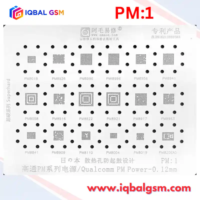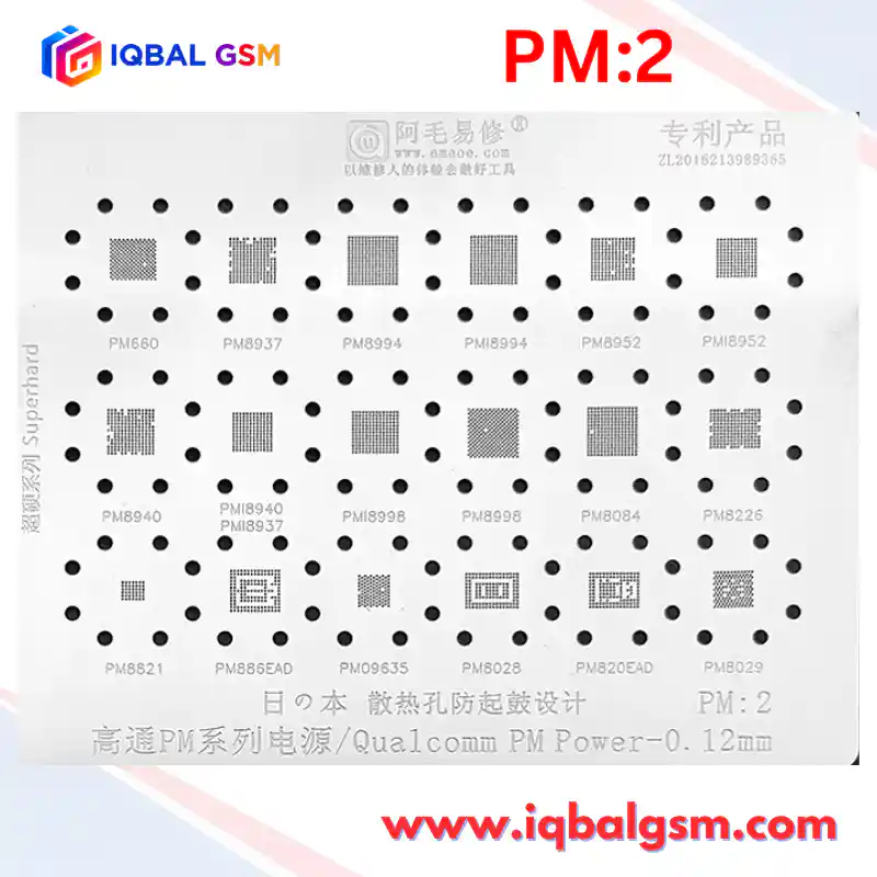

SU-2
As low as
Rs 700.00
Worldwide shipping · Cash on Delivery
Product Details
SPREADTRUM / UNISOC HARDWARE ARCHITECTURE & SILICON TOPOLOGY
1. MONOLITHIC SOC VS. MULTI-CHIP SYSTEM TOPOLOGY
- Monolithic Feature Phone Architecture (SC6531E / SC6531DA / SC6533G / SC6500D):
* Unlike high-end Qualcomm or MediaTek smartphone chipsets, Spreadtrum feature phone processors integrate the Application Processor (ARM926EJ-S), Baseband DSP, Analog RF Transceiver, Audio Class-D/AB Power Amplifier, Battery Charging Unit, and Power Management Unit (PMU) onto a single monolithic die or Multi-Chip Package (MCP) with co-packaged PSRAM (Pseudo-SRAM).
* Power input is routed directly from the battery connector (VBAT 3.7V - 4.2V) into the silicon. There is no external switching PMIC. The internal PMU converts VBAT into internal low-dropout supplies: VDD_CORE (1.1V - 1.2V), VDD_IO (1.8V / 2.8V), VDD_FLASH (2.8V - 3.0V), and VDD_RF (2.8V).
* Failure mode: Because VBAT enters the IC directly, electrical overstress (EOS) from faulty 5V chargers directly punctures the internal silicon power stage, producing a dead short across the battery terminals.
- Smart Smartphone / KaiOS Architecture (SC9850 / SC7731E / SC9820A):
* Uses a discrete 2-chip architecture: the Application Processor / Baseband SoC (SC9850 / SC7731E) paired with a dedicated companion PMIC (e.g., Spreadtrum SC2720 / SC2721 / SC2723G).
* The companion PMIC manages battery charging, supplies synchronous DC-DC buck regulators (VDD_CORE, VDD_CPU, VDD_MEM, VDD_IO), and coordinates with the AP via a dedicated serial power control bus.
2. SYSTEM BOOTSTRAP & CLOCK TIMING CHAIN
- Clock Generation:
* Master Reference Clock: 26.000 MHz Crystal Oscillator (XO). This clock is strictly mandatory for CPU boot, RF PLL lock, and USB interface enumeration. If the 26 MHz crystal is cracked or de-soldered, the IC draws micro-current and completely refuses to boot or enter download mode.
* Sleep Clock: 32.768 kHz RTC Crystal (or internally synthesized 32k RC oscillator in SC6531E). Keeps RTC, timer interrupts, and deep sleep low-power states active.
- Hardware Power-On Trigger (PWRKEY):
* The PWRKEY line is internally pulled up to VBAT (in feature phones) or VDD_IO 1.8V (in smartphones).
* When the user presses the Power button, PWRKEY is grounded (<0.3V).
* The internal PMU or companion PMIC debounces the signal for >150ms, releases the internal Power-On Reset (POR / RESET_N), and spins up the 26 MHz main clock.
- ROM Execution & SPD Flash Download Mode:
* The CPU begins executing internal BootROM.
* If the boot key (usually Center D-Pad Key, '*', or Boot Test Point) is held low while plugging in USB, the BootROM halts standard flash memory boot and activates the Spreadtrum Serial Protocol (Spreadtrum USB Download Mode).
* Device Manager enumerates the handset as: "SPRD U2S Diag" or "Spreadtrum ROM Device" (VID: 1782, PID: 4D00).
STEP-BY-STEP HOT AIR REWORK & REBALLING METHODOLOGY
1. DESOLDERING & THERMAL PROFILE MANAGEMENT
- Thin PCB Substrate Hazard:
* Budget handsets utilizing SC6531E, SC7731E, or SC9850 are constructed on thin 4-layer or 6-layer low-glass-transition-temperature (Tg) FR-4 circuit boards. These boards are extremely sensitive to heat and will blister, warp, or suffer internal ground-plane delamination if subjected to prolonged heating.
- Hot Air Extraction Settings:
* Nozzle: 5mm - 7mm circular nozzle.
* Station Settings: Temperature: 330°C - 340°C | Airflow: 40% - 45% (Quick 861DW benchmark).
* Shielding: Protect the adjacent SPI NOR flash (in feature phones) or eMMC / MCP (in smartphones) using high-temperature polyimide (Kapton) tape.
* Extraction: Apply a small ring of RMA-218 or NC-559-ASM rosin flux around the perimeter. Warm the board from a distance of 4cm in wide circular sweeps for 20 seconds. Focus hot air directly over the silicon die for 15-20 seconds. Touch the edge with fine tweezers. Once surface tension liquefies all solder balls, lift the IC vertically at a 90° angle. Never pull with mechanical force to prevent pad lift.
- PCB BGA Pad Preparation:
* Spread fresh leaded flux onto the site. Clean using a 1.5mm - 2.0mm copper desoldering wick under a micro-chisel soldering iron tip (T12-D16 or C210-020) at 320°C.
* Sweep gently until pads are completely flat and co-planar. Wipe clean with pure anhydrous isopropyl alcohol (IPA). Inspect the pad array under a microscope for severed solder mask webbing.
2. PRECISION REBALLING WITH AMAOE SU:2 STENCIL
- Solder Alloy Selection:
* Use Leaded Medium-Temperature Solder Paste: Sn63/Pb37 (Melting Point: 183°C).
* DO NOT use 138°C low-temperature bismuth alloy. Bismuth solder balls are mechanically brittle; when drop-tested, feature phones easily suffer fractured solder joints under the CPU. Furthermore, under RF transmission (GSM 900/1800 2W burst power), the integrated RF power amp on the monolithic die causes thermal cycling that fractures low-temp solder.
- Stencil Mounting & Paste Packing:
* Clean the AMAOE SU:2 plate with IPA. Seat the target chip into its corresponding engraved aperture (e.g., SC6531E, SC9850, or SC7731E).
* Check pad registration under 10x-20x magnification.
* Take a dime-sized amount of Sn63/Pb37 paste and squeegee it across oil-absorbent lens tissue until excess flux solvent is absorbed, transforming it into a matte, spreadable putty.
* Scrape the paste firmly into the stencil apertures using a stainless steel spatula held at a 45° angle. Scrape off the surface cleanly in a single sweep.
- Solder Ball Formation:
* Station Settings: Temperature: 280°C - 290°C | Airflow: 25% - 30% (Low airflow to avoid ball popping/blowaway).
* Direct the nozzle 3cm - 4cm above the plate. Warm the surrounding steel plate first to prevent localized thermal warping, then bring heat gradually over the apertures.
* Observe the gray paste melt and transform into uniform, gleaming solder spheres. Allow 10 seconds to solidify, then gently flex or push the chip from the underside to release it.
- Final Ball Finishing:
* Apply a micro-droplet of liquid flux onto the reballed balls.
* Reflow briefly with hot air at 280°C for 3 seconds. The balls will achieve perfect sphericity and uniform height.
3. MOTHERBOARD ALIGNMENT & SOLDERING
- Spread a micro-thin, uniform sheen of tacky flux over the cleaned motherboard footprint.
- Align the Pin 1 index dot on the processor package with the silkscreen bracket on the PCB.
- Hot Air Soldering Parameters:
* Temperature: 320°C - 330°C | Airflow: 35% - 40%.
* Heat perpendicularly in smooth circular loops around the chip boundary.
* When the solder reflows, the chip will sink slightly and self-center. Give one corner a microscopic tap with fine tweezers; the chip must instantly spring back into alignment via liquid surface tension.
- Allow the motherboard to cool naturally for 3 minutes before applying battery power.
COLD DIODE-MODE & DC POWER SUPPLY DIAGNOSTIC MATRIX
1. BENCH DC POWER SUPPLY CURRENT-CONSUMPTION PROFILES (3.8V - 4.0V VBAT HOOKUP)
- Profile A: Instant Short Circuit (0.000A -> 2.0A - 5.0A OCP Trip instantly on connection)
* Defect: Primary VBAT bus dead short.
* Root Cause: Common in SC6531E / SC6531DA monolithic chips where the internal battery charging MOSFET or ESD clamp diode has ruptured from high voltage.
* Diagnostic Step: Inject 1.5V / 2A onto VBAT terminals with rosin vapor or thermal imaging. If the SC6531E chip body heats up immediately, the CPU is internally shorted and must be replaced.
- Profile B: Absolute Zero Current on Power Key (0.000A Static)
* Defect: Power-on signal line broken or standby circuit open.
* Root Cause: Broken trace on PWRKEY line (open circuit to button contact pad); dead 26.000 MHz main crystal; missing internal LDO bias; cracked solder ball on VBAT input balls.
- Profile C: Micro-Current Freeze (0.015A - 0.035A Fixed Current)
* Defect: Power trigger initiates, but processor clock or Core Buck fails to run.
* Root Cause: 26 MHz crystal failed / open ground capacitors; short circuit on VDD_CORE (1.1V); broken solder joint on RESET_N.
- Profile D: Medium Current Bootloop (Pulses 0.040A -> 0.090A -> Drops to 0.000A -> Loops)
* Defect: BootROM initializes, but fails to read SPI NOR Flash (in feature phones) or eMMC (in smartphones).
* Root Cause: Desoldered / corrupted SPI flash IC (common in dropped feature phones); missing VDD_FLASH (2.8V - 3.0V) power supply; solder bridge across SPI data lines (SPI_CLK, SPI_CS, SPI_SI, SPI_SO).
- Profile E: USB Download Mode Enumeration Test
* Action: Hold Boot Key (or short Boot test point to GND) and plug in USB to PC.
* Result: If current jumps to a stable 0.060A - 0.080A and PC detects "SPRD U2S Diag", the CPU silicon, internal PMU, 26 MHz clock, and USB PHY are 100% functional; the fault is strictly corrupted firmware or a damaged Flash/eMMC storage chip.
2. COLD DIODE-MODE IMPEDANCE BENCHMARKS (RED PROBE TO GROUND, BLACK PROBE TO TARGET PIN/TEST POINT)
- Standard Diode Readings for Spreadtrum / UNISOC Platforms (SC6531E / SC7731E):
* VBAT Battery Connector Positive : 0.420V - 0.520V (If <0.150V: Primary battery bus shorted)
* VDD_CORE Supply Capacitor : 0.220V - 0.320V (If 0.000V: CPU internal logic shorted)
* VDD_IO / VDD18 (1.8V Rail) : 0.380V - 0.460V (If <0.180V: Peripheral bus shorted)
* VDD_FLASH / VDD28 (2.8V Rail) : 0.450V - 0.530V (If OL: Broken circuit to internal LDO)
* 26.000 MHz Crystal Pin 1 (OSC_IN): 0.560V - 0.650V (If OL: Trace disconnect to CPU)
* 26.000 MHz Crystal Pin 3 (OSC_OUT): 0.560V - 0.650V (Must match OSC_IN within 15mV)
* PWRKEY Power Button Pad : 0.580V - 0.720V (If OL: Broken trace from key pad to CPU)
* USB_DP (Data +) Pin : 0.540V - 0.640V (Must be closely balanced with USB_DN)
* USB_DN (Data -) Pin : 0.540V - 0.640V (If unbalanced >50mV: CPU USB PHY damaged)
* SPI_CLK / SPI_CS Flash Lines : 0.480V - 0.560V (If 0.000V: Bus shorted; prevents boot)