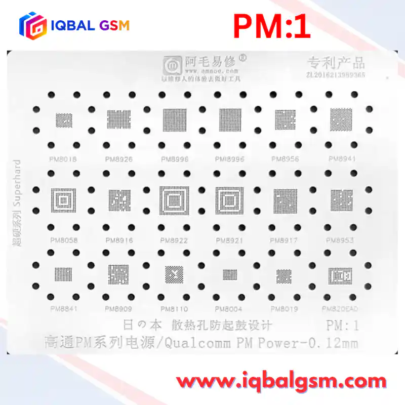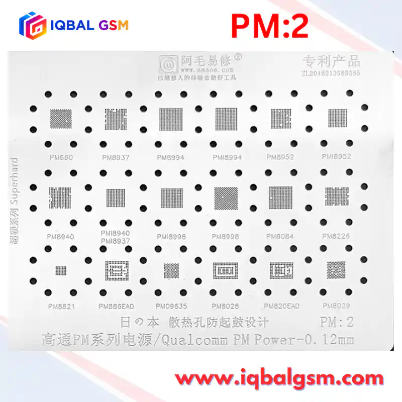

SU-1
As low as
Rs 700.00
Worldwide shipping · Cash on Delivery
Product Details
SPREADTRUM / UNISOC HARDWARE ARCHITECTURE & SILICON POWER TOPOLOGY
1. POWER TREE ARCHITECTURE: APPLICATION PROCESSOR & DEDICATED COMPANION PMIC
- Unlike monolithic feature phone SoCs, the Spreadtrum SC9830A, SC9832A, and SC7731/8830 platforms utilize a discrete 2-chip power distribution architecture paired with dedicated companion PMICs (e.g., Spreadtrum SC2723G, SC2723, SC2721G, or SC2713):
* Companion PMIC (SC2723G / SC2721G):
Houses the switching battery charger, fuel gauge logic, multi-phase synchronous buck converters (VDD_CORE, VDD_CPU, VDD_MEM, VDD_IO), auxiliary LDO regulators (VDD_EMMC, VDD_CAM, VDD_SENSORS), and audio codec/PA circuitry.
* Application Processor (SC9830A / SC7731 / SC8830):
Contains the Cortex-A7 CPU cluster, Mali GPU, Baseband DSP engines, memory controller, and high-speed peripheral interfaces.
- Power Domain Rails:
* VDD_CORE (0.95V - 1.15V Dynamic VID): Powers the digital baseband core and internal system logic.
* VDD_CPU (1.00V - 1.25V Dynamic VID): Dynamic voltage rail for the Quad Cortex-A7 cluster.
* VDD_MEM (1.20V LPDDR2 / 1.10V LPDDR3): Core voltage rail for external or MCP-packaged SDRAM.
* VDD_1P8 (1.80V Fixed): Standard peripheral IO rail, SPMI/I2C communication, and clock buffers.
* VDD_EMMC / VCC (2.85V - 3.00V): Storage flash NAND array supply.
2. CLOCK DISTRIBUTION, BOOT SEQUENCE & TIMING BENCHMARK
- Dual Clock Generation Chain:
* Master Reference Clock (26.000 MHz): Sourced from a discrete temperature-compensated crystal (TCXO) or 26 MHz quartz crystal. CRITICAL: In Spreadtrum architectures, the 26 MHz clock is strictly mandatory to run the internal PLLs, BootROM sequencer, and USB transceiver. If the 26 MHz crystal fails or has cold solder joints, the phone will show 0.000A or a static 0.020A current freeze and will never communicate over USB.
* Real-Time Clock (32.768 kHz): Sourced from an external RTC tuning fork crystal or synthesized internally by the PMIC. Powers the low-power sleep state machine and watchdog timers.
- Power-On Handshake Sequence:
* Stage 1: VBAT (3.7V - 4.2V) enters the PMIC (SC2723G). Internal standby LDOs generate VDD_AO_1P8.
* Stage 2: Power key is pressed, pulling PWRKEY_N low (<0.4V) for >150ms.
* Stage 3: PMIC triggers the internal power-on sequencer. Synchronous bucks initialize in strict order: VDD_CORE -> VDD_MEM -> VDD_CPU -> VDD_IO.
* Stage 4: PMIC turns on the 26 MHz crystal oscillator buffer and asserts RESET_N (1.8V) high to release the SC9830A CPU from reset.
* Stage 5: CPU executes primary BootROM. Within 500ms, the CPU must pull PS_HOLD (1.8V) high back to the PMIC. If PS_HOLD fails to latch, the PMIC cuts all buck lines and restarts (bootlooping signature).
STEP-BY-STEP HOT AIR REWORK & REBALLING METHODOLOGY
1. CHIP DESOLDERING & SUBSTRATE PROTECTION
- Low-Tg Board Substrate Warning:
* Handsets using SC9830A, SC7731, or SC8830 (e.g., Samsung Galaxy J1, J3, Grand Prime, Core Prime) are built on budget 4-layer or 6-layer FR-4 printed circuit boards. These boards have low glass-transition temperatures (Tg ~130°C - 140°C). Heating for more than 40 continuous seconds will cause the PCB substrate to blister, pop-corn, or tear internal ground vias.
- Shielding & Hot Air Extraction Parameters:
* Thermal Shield: Wrap adjacent eMMC flash memory, RF transceivers, and plastic camera/battery connectors in dual-layer polyimide (Kapton) tape backed with 0.1mm aluminum or copper foil.
* Hot Air Station Settings: Temperature: 335°C - 345°C | Airflow: 45% - 50% (Quick 861DW benchmark).
* Extraction Technique: Apply high-grade RMA-218 or NC-559-ASM flux around the SoC edges. Pre-heat the entire PCB quadrant in wide spiral circles (3cm radius) for 25 seconds. Bring nozzle directly over the SoC package at a distance of 2cm. Maintain continuous, small circular movements.
* Release: Test the corner of the SoC with ultra-fine curved tweezers. Once molten surface tension is reached, lift the chip vertically at a 90° angle. NEVER force or pry the chip; doing so will rip copper pads from the PCB.
- Motherboard BGA Site Preparation:
* Add leaded rosin flux and use a 2.0mm copper desoldering wick under a soldering iron chisel tip (T12-D24 / C210-020) set to 320°C - 330°C.
* Gently sweep across the pad array until all residual solder mounds are removed and pads are completely flat. Wipe clean with pure anhydrous isopropyl alcohol (IPA). Inspect under a microscope for lifted pads or compromised solder resist webbing.
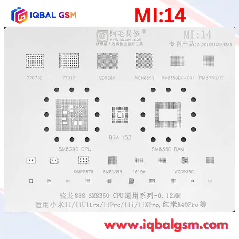
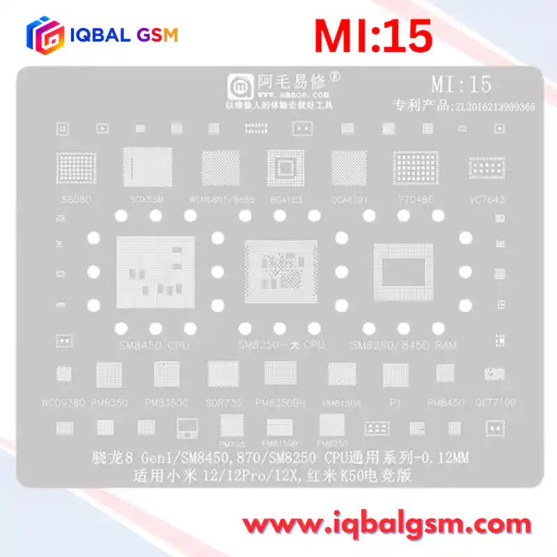
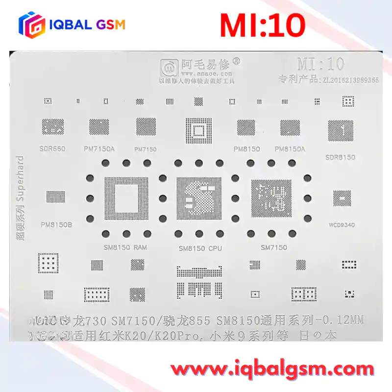
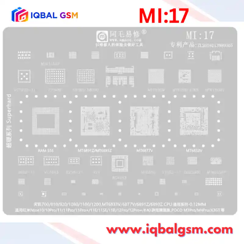
2. PRECISION REBALLING WITH AMAOE SU:1 STENCIL
- Solder Alloy Selection:
* Use Leaded Medium-Temperature Solder Paste: Sn63/Pb37 (Melting Point: 183°C).
* DO NOT use low-temperature bismuth alloy (138°C Sn42/Bi58). The SC9830A / SC7731 processors run under sustained high-load thermal cycling (Mali GPU gaming and 4G LTE transmission), easily reaching junction temperatures of 70°C - 85°C. At these temperatures, bismuth solder joints soften, undergo rapid electromigration, crack, and fail drop tests.
- Stencil Registration & Paste Preparation:
* Mount the cleaned processor into its designated aperture on the AMAOE SU:1 stencil plate.
* Align all BGA pad holes under 10x-20x magnification. Ensure the stencil plate lies 100% planar against the silicon substrate.
* Place a dollop of Sn63/Pb37 solder paste onto lint-free lens paper. Squeegee firmly with a flat spatula to absorb excess flux solvent until the paste achieves a thick, matte, putty-like consistency.
* Scrape paste into the apertures at a 45° angle. Ensure every aperture is 100% filled. Wipe the stencil top clean in a single diagonal pass.
- Solder Ball Formation:
* Station Settings: Temperature: 280°C - 290°C | Airflow: 25% - 30% (Low airflow to prevent ball blow-off).
* Direct the nozzle 3cm - 4cm above the stencil. Warm the steel plate around the perimeter first to relieve thermal expansion stress, then sweep smoothly across the apertures.
* Watch the paste liquefy into bright, gleaming spherical balls. Allow 10 seconds of passive cooling, then release the chip from the stencil underside using ESD tweezers.
- Secondary Finishing Reflow:
* Apply a micro-droplet of liquid flux across the reballed spheres.
* Reflow with hot air at 280°C for 3 seconds. Surface tension will pull every solder ball into a perfectly uniform, gleaming spherical shape.
3. MOTHERBOARD SOLDERING & ALIGNMENT
- Dispense a micro-thin, uniform film of high-tack leaded flux onto the motherboard footprint.
- Align the Pin 1 orientation marker (laser dot on SoC package corner) with the silkscreen bracket on the PCB.
- Hot Air Soldering Parameters:
* Temperature: 325°C - 335°C | Airflow: 40%.
* Heat in wide, continuous loops around the chip perimeter, gradually moving inward.
* As the solder balls melt, the chip will sink slightly and self-align. Give one corner of the die a microscopic nudge with fine tweezers (<0.2mm lateral displacement); if properly soldered, the chip will instantly spring back to center via liquid surface tension.
- Allow the motherboard to cool naturally for 3 minutes before connecting bench power.
COLD DIODE-MODE & DC POWER SUPPLY DIAGNOSTIC MATRIX
1. BENCH DC POWER SUPPLY CURRENT-CONSUMPTION PROFILES (3.8V - 4.0V VBAT HOOKUP)
- Profile 1: Primary Dead Short (0.000A -> Instant Over-Current Protection Trip @ 2.0A - 5.0A)
* Defect: Primary VBAT bus dead short to ground.
* Root Cause: Shorted high-side buck MOSFET inside the companion PMIC (SC2723G / SC2721G), or ruptured 22uF ceramic decoupling capacitor on the VBAT / VPH line.
* Action: Connect DC supply at 1.2V / 3A with a thermal camera. If the companion PMIC glows instantly at low voltage, the PMIC is internally bridged and must be replaced.
- Profile 2: Total Zero Current Draw on Power Key Press (0.000A Static)
* Defect: Power-on trigger circuit open or standby voltage missing.
* Root Cause: Broken trace on PWRKEY line (PWRKEY missing 1.8V / VBAT pull-up); defective 32.768 kHz RTC oscillator; open circuit on PMIC VBAT feed pins; cracked solder ball under PMIC power input.
- Profile 3: Micro-Current Freeze (0.015A - 0.040A Constant Draw)
* Defect: PMIC initiates power-up, but processor core clock or digital logic fails to execute.
* Root Cause: Defective 26.000 MHz Master Crystal (XO); missing VDD_CORE (1.0V) or shorted core filter capacitor; cracked solder ball on RESET_N line between PMIC and SC9830A.
- Profile 4: Medium Current Bootloop (Pulses 0.060A -> 0.160A -> Drops to 0.000A -> Repeats)
* Defect: Missing PS_HOLD handshake from the SC9830A processor.
* Root Cause: PMIC generates all buck rails and asserts RESET_N, but processor cannot read BootROM / eMMC bootloader due to missing VDD_EMMC / VDD_MEM rails, corrupted eMMC flash partition, or cracked BGA balls under the eMMC storage chip.
- Profile 5: Spreadtrum USB Download Mode (SPRD U2S Diag) Verification
* Test Procedure: Hold Volume Down / Boot Key and plug the phone into a PC via USB.
* Result: If current latches at a stable 0.050A - 0.075A and Windows Device Manager enumerates "SPRD U2S Diag" or "Spreadtrum ROM Device" (VID: 1782, PID: 4D00), the SC9830A CPU, internal USB PHY, 26 MHz reference clock, and PMIC buck stages are 100% operational; the defect is strictly corrupted firmware or a failed eMMC memory chip.
2. COLD DIODE-MODE IMPEDANCE MATRIX (RED PROBE TO GROUND, BLACK PROBE TO TARGET PIN/TEST POINT)
- Baseline Diode Readings for Spreadtrum SC9830A / SC8830 / SC7731 Power Nodes:
* VBAT Main Power Input : 0.400V - 0.500V (If <0.150V: Primary battery bus shorted)
* VDD_CORE Buck Inductor (1.0V) : 0.150V - 0.240V (Low baseline diode drop is normal for core logic)
* VDD_CPU Buck Inductor (1.1V) : 0.140V - 0.220V (If 0.000V: CPU silicon core shorted)
* VDD_MEM LPDDR Rail (Inductor) : 0.280V - 0.360V (If <0.120V: RAM die compromised)
* VDD_1P8 IO Rail (Inductor/Cap) : 0.380V - 0.460V (If <0.200V: Peripheral bus shorted)
* VDD_EMMC Flash Supply (2.85V) : 0.450V - 0.530V (If OL: Trace break from PMIC LDO)
* 26.000 MHz Crystal Pin 1 (OSC_IN): 0.540V - 0.640V (If OL: Broken trace to SC9830A ball)
* 26.000 MHz Crystal Pin 3 (OSC_OUT): 0.540V - 0.640V (Must match OSC_IN within 15mV)
* PWRKEY Power Button Pad : 0.580V - 0.700V (If OL: Trace disconnect to PMIC)
* PS_HOLD Line : 0.420V - 0.500V (If 0.000V: CPU PS_HOLD pin shorted to ground)
* USB_DP (Data +) Pin : 0.520V - 0.620V (Balanced with USB_DN within 10mV)
* USB_DN (Data -) Pin : 0.520V - 0.620V (If unbalanced >50mV: CPU USB PHY damaged)