
RF-1
As low as
Rs 700.00
Worldwide shipping · Cash on Delivery
Product Details
MOBILE RF FRONT-END (RFFE) POWER AMPLIFIER ARCHITECTURE & REPAIR TOPOLOGY
1. POWER AMPLIFIER (PA) & PAMID OPERATING PHYSICS & CIRCUIT TOPOLOGY
- In modern multi-mode 4G and 5G smartphones, the RF Power Amplifier is the highest current-consuming component outside the CPU:
* PAMiD (Power Amplifier Module with integrated Duplexers):
Combines GaAs (Gallium Arsenide) / GaN (Gallium Nitride) high-electron-mobility RF transistors, CMOS bias controllers, SOI (Silicon-on-Insulator) antenna switches, and surface acoustic wave (SAW) / bulk acoustic wave (BAW) duplexer filters into a single compact, high-density land grid array (LGA) package.
* Dual-Power Delivery Rails:
- VCC1 / VCC2 (Main Power Supply): Fed directly from VBAT (3.4V - 4.4V) or from an external Average Power Tracking (APT) / Envelope Tracking (ET) dynamic DC-DC buck converter (e.g., Qualcomm QET-series, Samsung Shannon-ET). Under 5G NR uplink transmission or 2G GSM burst mode (2W peak power), the PA draws 2.0A - 2.8A of instantaneous transient current.
- VDD_IO (1.80V): Powers internal CMOS control logic and MIPI RFFE bus interfaces.
* Control Bus (MIPI RFFE v2.0 / v2.1):
The Baseband / Transceiver controls power levels, band selection, and bias current via the bidirectional MIPI Radio Frequency Front-End bus (RFFE_CLK, RFFE_DATA, and VIO 1.8V). A broken RFFE trace locks the PA in an unconfigured state, causing "No Service" or immediate network drop.
- High-Frequency Failure Modes:
* Mode A (Direct VBAT Short / Dead Board): Electrical overstress (EOS) from voltage spikes punctures the internal GaAs collector-emitter junctions, shorting the primary VBAT rail directly to ground. The phone refuses to power on and trips bench DC supply over-current protection (2.0A - 5.0A).
* Mode B (Call-Initiated Power Cut / Instant Reboot): Under idle standby, the PA is un-biased and draws <5mA. When a cellular voice call is dialed or high-speed 4G/5G data uploads begin, the baseband asserts PA_EN; the damaged internal power stage breaks down under RF drive, pulling VBAT below 3.3V and triggering system PMIC Under-Voltage Lockout (UVLO).
* Mode C (No Service / Weak Signal / Searching): Fractured BGA solder joints on the antenna TX/RX pins or central ground plane caused by physical drop shock. The phone shows full Wi-Fi, but cannot register on cellular towers.
STEP-BY-STEP HOT AIR REWORK & REBALLING METHODOLOGY
1. CHIP REMOVAL & MOTHERBOARD SITE PREPARATION
- Thermal Protection:
* RF Power Amplifiers are situated inside heavily shielded RF compartments immediately adjacent to the RF transceiver (SDR / Shannon / MT6177), sensitive SAW filters, and high-frequency coaxial antenna connectors.
* Apply dual-layer thermal shielding: high-temperature polyimide (Kapton) tape topped with 0.1mm adhesive copper foil over all adjacent RF transceiver ICs, crystal oscillators, and plastic coax sockets.
- Hot Air Extraction Settings:
* Nozzle: 5mm - 6mm circular nozzle.
* Station Settings: Temperature: 335°C - 345°C | Airflow: 40% - 45% (Quick 861DW benchmark).
* Pre-Heating Technique: RF power amplifiers sit on thick multi-layer copper ground planes designed to conduct heat away from the silicon. Apply RMA-218 or NC-559 flux around the package perimeter. Pre-heat the entire RF shield area in wide spiral loops for 25-30 seconds to bring the heavy ground planes to 180°C.
* Extraction: Bring nozzle 2cm above the PA package in continuous circular motion. Touch the corner of the chip gently with ultra-fine tweezers. Once the large central ground solder slug liquefies completely, lift the IC vertically at a 90° angle. NEVER pry or wrench the chip; pulling before the central ground pad melts will tear ground copper planes directly off the PCB.
- PCB BGA Pad Planarization:
* Add leaded rosin flux and use a 2.0mm copper desoldering wick under a soldering iron chisel tip (T12-D24 / C210-020) set to 330°C.
* Flatten the central ground slug and perimeter LGA pads until 100% planar. Clean thoroughly with pure anhydrous isopropyl alcohol (IPA) and an ESD brush. Inspect under stereo microscope for solder bridges or damaged solder mask between signal pins and ground.
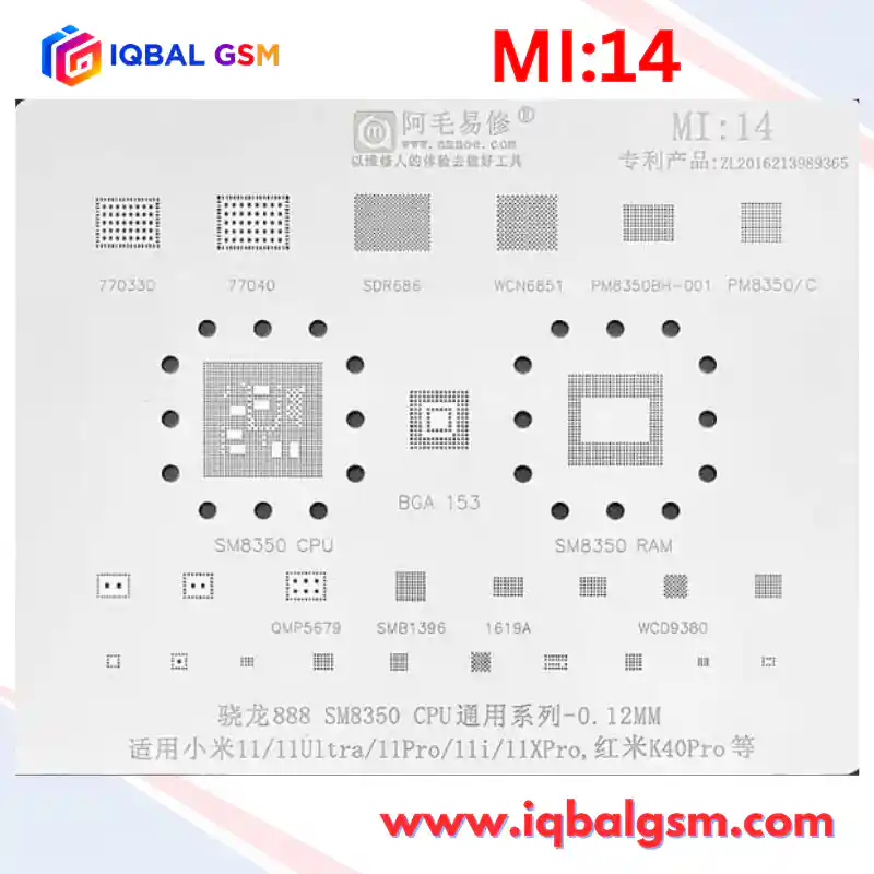
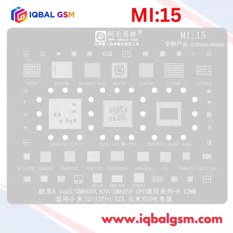
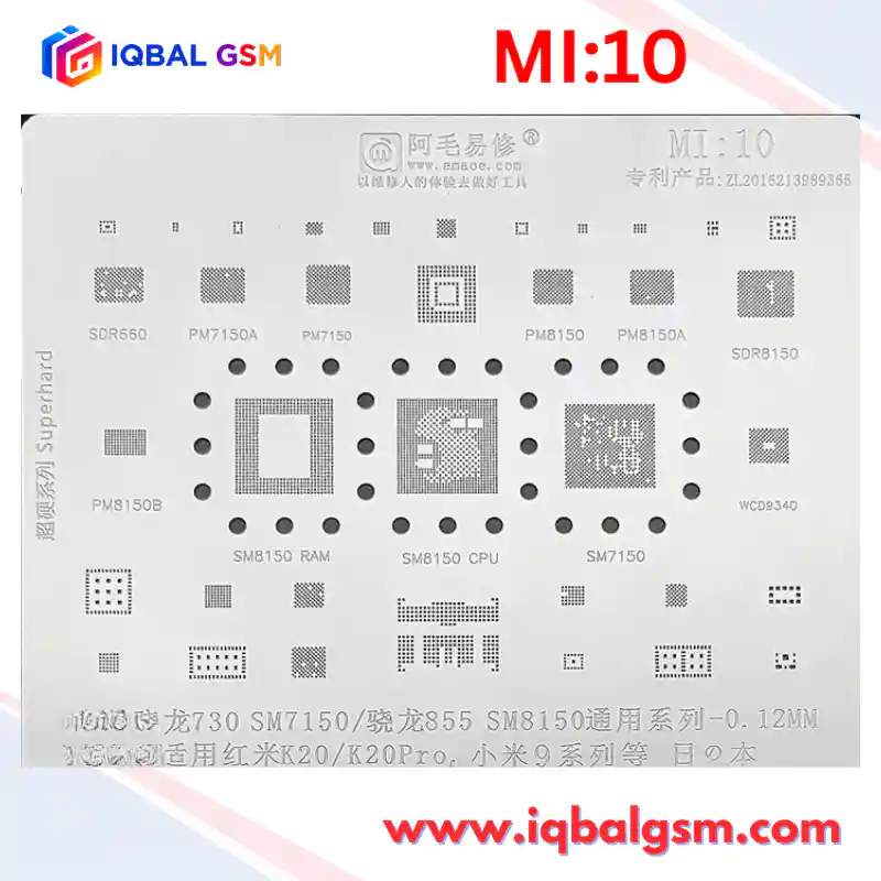
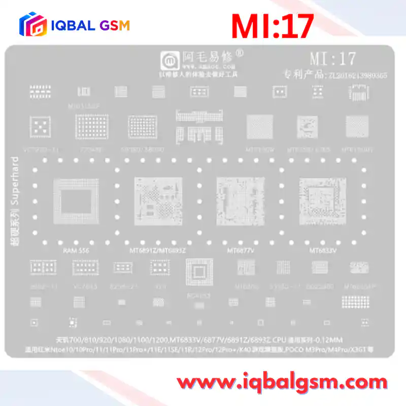
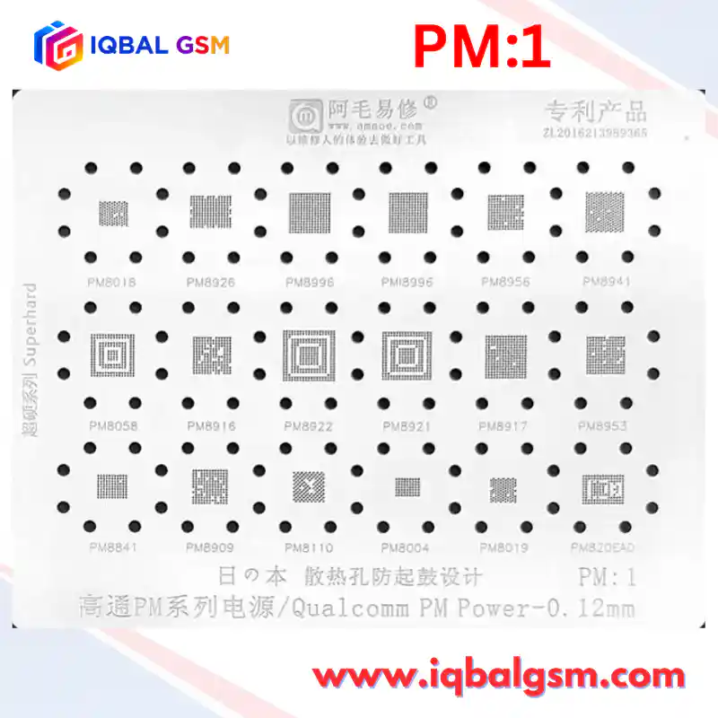
2. PRECISION REBALLING WITH AMAOE RF:1 STENCIL
- Solder Alloy Selection (CRITICAL RULE):
* Use Medium-Temperature Leaded Solder Paste: Sn63/Pb37 (Melting Point: 183°C).
* STRICT WARNING: NEVER use 138°C low-temperature bismuth alloy (Sn42/Bi58) on RF Power Amplifiers. During 5G high-power transmissions (Power Class 2 / +26dBm) or 2G GSM bursts, power amplifier internal junction temperatures easily reach 85°C - 105°C. At these temperatures, 138°C bismuth solder softens, suffers rapid electromigration, cracks, and creates catastrophic solder bridging across the high-voltage supply lines.
- Stencil Registration & Paste Preparation:
* Mount the cleaned PA chip (e.g., SKY78191, QPM5677, SKY77656, or HI6D21) into its corresponding engraved aperture on the AMAOE RF:1 plate.
* Align all micro-pad apertures under 10x-20x magnification. Ensure the stencil plate lies 100% flat against the component.
* Place a dollop of Sn63/Pb37 solder paste onto lint-free lens paper and squeeze firmly with a spatula to absorb excess flux solvent until the paste achieves a matte, putty-like consistency.
* Scrape paste firmly into the apertures using a stainless steel squeegee held at a 45° angle. Scrape surface clean in a single diagonal stroke.
- Solder Ball Formation:
* Station Settings: Temperature: 280°C - 290°C | Airflow: 25% - 30% (Low airflow prevents ball popping/blowaway).
* Direct nozzle 3cm - 4cm above the plate. Warm the surrounding steel plate first to relieve thermal stress, then sweep smoothly across the aperture grid.
* Watch the paste melt into gleaming spherical balls. Allow 10 seconds to cool, then release the chip from the stencil underside using ESD tweezers.
- Secondary Finishing Reflow:
* Apply a micro-droplet of liquid flux over the reballed spheres.
* Reflow with hot air at 280°C for 3 seconds. Surface tension will pull every solder ball into a perfectly uniform, gleaming spherical shape.
3. MOTHERBOARD SOLDERING & ALIGNMENT
- Dispense a micro-thin, uniform sheen of high-tack flux across the motherboard footprint.
- Align the Pin 1 orientation index (laser dot on PA package corner) with the silkscreen bracket on the PCB.
- Hot Air Soldering Parameters:
* Temperature: 325°C - 335°C | Airflow: 35% - 40%.
* Heat in smooth circular loops around the chip boundary. Because the central ground pad requires significant thermal energy to melt, maintain heat until the chip visibly sinks and self-aligns.
* Give one corner of the package a microscopic nudge with fine tweezers (<0.2mm displacement); the IC will immediately spring back to center position via liquid surface tension.
- Allow the motherboard to cool naturally for 3 minutes before applying battery power.
COLD DIODE-MODE & DC BENCH SUPPLY DIAGNOSTIC MATRIX
1. BENCH DC POWER SUPPLY CURRENT SIGNATURES (4.0V VBAT HOOKUP)
- Fault Signature 1: Direct Dead Short (0.000A -> Instant Over-Current Trip @ 2.0A - 5.0A)
* Defect: Primary VBAT bus dead short to ground.
* Root Cause: High-side GaAs/CMOS power transistor breakdown inside the PA (e.g., SKY77643, SKY78191, QPM5677), or shorted 22uF ceramic decoupling capacitor on the PA VBAT line.
* Diagnostic Step: Inject 1.5V / 3A on VBAT with a thermal camera. If the PA package glows white-hot instantly at low voltage, remove the PA; if short clears, replace the PA.
- Fault Signature 2: Call-Initiated Shutoff (Boots Normally, Drops to 0.000A Upon Dialing Voice Call)
* Defect: PA internal silicon breakdown under dynamic RF power amplification.
* Root Cause: The PA functions normally during low-power RX reception, but when Baseband asserts PA_EN for high-power TX uplink, internal current spikes exceed 3.0A, dropping VBAT below 3.3V and forcing system PMIC into Under-Voltage Lockout (UVLO).
- Fault Signature 3: High Standby Leakage Current (Static 0.350A - 0.650A Warmth in RF Can)
* Defect: Leaky internal bias regulator inside the PAMiD module.
* Root Cause: Partial dielectric puncture inside the PA CMOS bias block holding internal gates partially open in idle mode.
- Fault Signature 4: "No Service" / "Searching..." with Normal Boot Current (0.150A - 0.250A)
* Defect: Transmit/Receive path open circuit or missing MIPI RFFE control communication.
* Root Cause: Cracked solder joints under PA antenna switch pins, open circuit on MIPI_RFFE_DATA / MIPI_RFFE_CLK lines, or missing VIO 1.8V logic supply.
2. COLD DIODE-MODE IMPEDANCE BENCHMARKS (RED PROBE TO GROUND, BLACK PROBE TO TARGET PIN/CAPACITOR)
- Standard Diode Readings for Skyworks / Qualcomm / HiSilicon PA Modules (SKY78191 / QPM5677 / SKY77656):
* VBAT / VCC_PA Power Input Pin : 0.380V - 0.460V (If <0.100V: Primary RF power stage shorted)
* VIO 1.8V Logic Supply Pin : 0.380V - 0.460V (If <0.180V: MIPI bus logic supply shorted)
* MIPI_RFFE_CLK Line : 0.440V - 0.520V (If OL: Broken trace from Baseband processor)
* MIPI_RFFE_DATA Line : 0.440V - 0.520V (Must match CLK within 15mV; if 0.000V: Bus shorted)
* RF_IN (Transceiver TX Input) : 0.320V - 0.400V (If OL: Inter-stage coupling capacitor cracked)
* RF_OUT / ANT Port (Antenna Pin) : 0.450V - 0.550V (If 0.000V: Antenna switch or ESD diode shorted)
* PA_ENABLE / APT_ENABLE Pin : 0.520V - 0.620V (If OL: Broken control trace from transceiver)
* Central Thermal Ground Slug : 0.000V - 0.001V (Direct low-impedance ground return)