
SAM-13
As low as
Rs 700.00
Worldwide shipping · Cash on Delivery
Product Details
SAMSUNG GALAXY A-SERIES HYBRID HARDWARE ARCHITECTURE & SILICON TOPOLOGY
1. DUAL-ECOSYSTEM POWER DISTRIBUTION: QUALCOMM SPMI VS. MEDIATEK I2C TOPOLOGY
- The AMAOE SAM:13 stencil services both Qualcomm-based and MediaTek-based Samsung Galaxy A-series handsets:
* Qualcomm Snapdragon 675 / SM6150 Architecture (Galaxy A70 / A60):
- Master PMIC (PM6150): Connected directly to VPH_PWR (3.6V - 4.2V). Generates Always-On standby supplies (VDD_AO_1P8, VDD_AO_0P8), houses the 19.200 MHz / 38.400 MHz Master CXO crystal oscillator buffer, 32.768 kHz RTC clock, and multi-phase synchronous buck converters: VDD_APC0 (Kryo 460 Gold cores dynamic VID 0.65V - 1.15V), VDD_APC1 (Kryo 460 Silver cores), VDD_MEM (1.125V LPDDR4X), and VDD_IO (1.80V).
- Secondary PMIC (PM6150A / PM6150L): Houses the switching battery charger (25W USB-PD / Samsung Super Fast Charging), AMOLED display bias supplies (+/-4.6V VDD_DISP / VEE_DISP), torch/flash LED drivers, and OTG 5V boost converter.
- SPMI Control Bus: The SM6150 CPU communicates with PM6150/PM6150A via Qualcomm's 2-wire SPMI bus (SPMI_CLK / SPMI_DATA) at 19.2 MHz. A cold solder joint or trace open causes an immediate shutdown or 0.030A current freeze.
* MediaTek Helio P22 / MT6762 Architecture (Galaxy A10s):
- Master PMIC (MT6357CRV): Directly accepts VBAT (3.7V - 4.2V). Contains the switching battery charger, fuel gauge, 26.000 MHz system clock driver, and integrated DC-DC bucks:
* VPROC (CPU core dynamic VID 0.70V - 1.15V)
* VCORE (digital logic and GPU core 0.80V)
* VIO18 (system IO 1.80V)
* VIO28 / VEMMC (storage flash NAND 3.00V)
- Control Interface: S2C / I2C serial control bus between MT6762 and MT6357CRV.
2. BOOT SEQUENCE & TIMING BENCHMARK
- Qualcomm SM6150 / Galaxy A70 Sequence:
* Step 1: VPH_PWR generated by PM6150L buck-boost converter from battery or USB charger.
* Step 2: PM6150 activates Always-On standby rails (VDD_AO_1P8). PWR_KEY_N pulled up to 1.8V.
* Step 3: Power key pressed (<0.4V for >120ms); PM6150 turns on 19.2 MHz Master CXO crystal buffer and asserts CXO_EN.
* Step 4: Synchronous bucks initialize: VDD_DIG (0.85V) -> VDD_MEM (1.125V) -> VDD_APC0/1 -> VDD_IO (1.8V).
* Step 5: Peripheral LDOs stabilize; PM6150 releases RESET_N (1.8V) to SM6150 CPU. CPU loads PBL from eMMC/UFS and returns PS_HOLD (1.8V) high within 500ms.
- MediaTek MT6762 / Galaxy A10s Sequence:
* Step 1: Direct VBAT connects to MT6357CRV. Standby LDOs fire (VPA, VRTC 1.8V, VIO18).
* Step 2: Power key pressed; MT6357CRV activates 26.000 MHz master crystal and ramps up VCORE (0.8V) and VPROC (0.9V).
* Step 3: MT6357CRV asserts SYSRSTB (1.8V) high to release MT6762 CPU.
* Step 4: MT6762 executes internal Preloader from eMMC flash storage and pulls WATCHDOG / PMIC_EN high to maintain power latch.
STEP-BY-STEP HOT AIR REWORK & REBALLING METHODOLOGY
1. UNDERFILL REMOVAL & CHIP EXTRACTION
- Thermal Protection:
* Mid-range Galaxy A-series boards use cost-optimized 6-layer or 8-layer circuit boards. Cover adjacent eMMC/UFS storage, battery FPC connectors, and microphones with dual-layer polyimide (Kapton) tape backed by 0.1mm adhesive copper foil.
- Underfill Edge Cleaning:
* Clamp motherboard in a CNC multi-axis repair fixture. Set hot air station to 230°C - 240°C with 35% airflow.
* Use a precision 0.1mm curved dental scraping probe to remove the perimeter underfill fillet around the target processor (SM6150 or MT6762) and surrounding 0201 decoupling capacitors. Do NOT apply lateral leverage against the PCB surface to avoid tearing top-layer ground copper.
- Hot Air Extraction Parameters:
* Apply RMA-218 or NC-559 flux around chip perimeter. Set hot air station to 340°C - 350°C (Quick 861DW benchmark, 45% airflow).
* Pre-heat the entire PCB area within a 3cm radius for 25 seconds using wide circular sweeps. Focus airflow directly over the processor package for 20 seconds.
* Test the edge of the CPU with ultra-fine curved tweezers. Once molten surface tension is confirmed, lift the chip vertically at a 90° angle. Never pry an un-melted chip.
- Motherboard Pad Planarization:
* Add leaded rosin flux and use a 2.5mm copper desoldering wick under a soldering iron chisel tip (T12-D24 / C210-020) set to 330°C.
* Sweep lightly across the pad array until all residual lead-free solder is removed and pads are perfectly planar. Wipe clean with pure anhydrous isopropyl alcohol (IPA). Inspect under stereo microscope for pad oxidation or torn solder mask webbing.
2. PRECISION REBALLING WITH AMAOE SAM:13 STENCIL
- Solder Alloy Selection:
* Use Medium-Temperature Leaded Solder Paste: Sn63/Pb37 (Melting Point: 183°C).
* DO NOT use 138°C low-temperature bismuth alloy. Both Qualcomm SM6150 and MediaTek MT6762 processors dissipate continuous thermal loads during gaming and GPS navigation. Bismuth solder joints soften, undergo rapid electromigration, and crack under physical drop shock.
- Stencil Registration & Paste Packing:
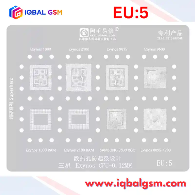
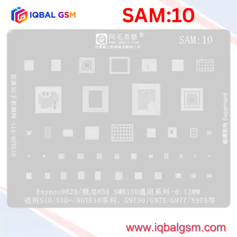
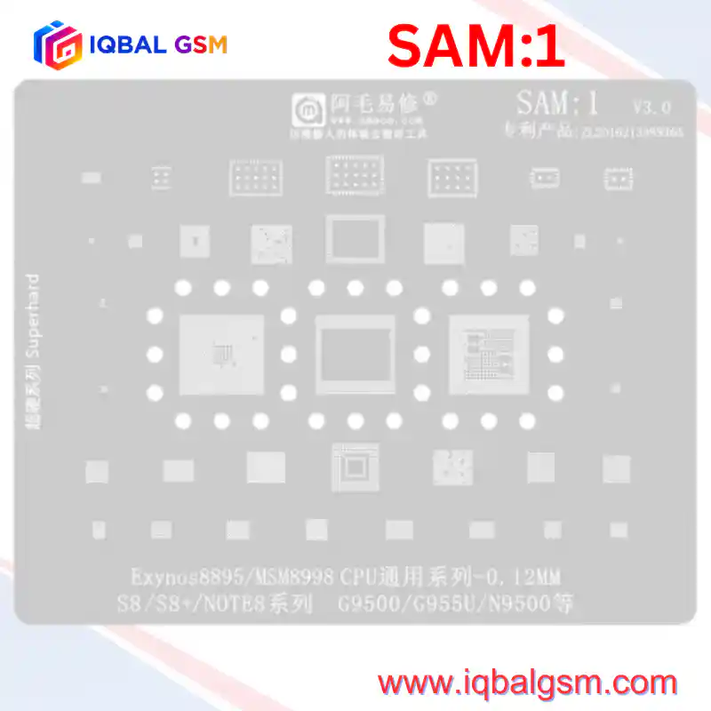
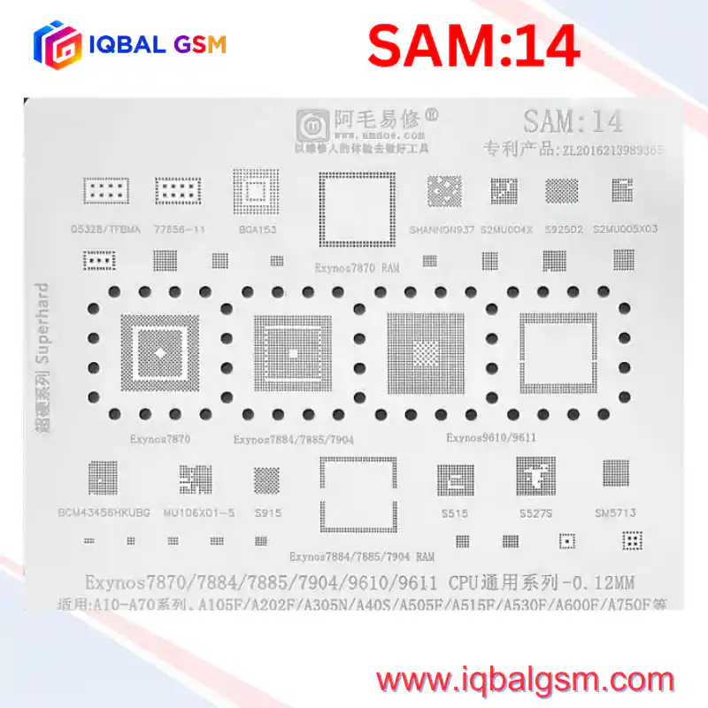
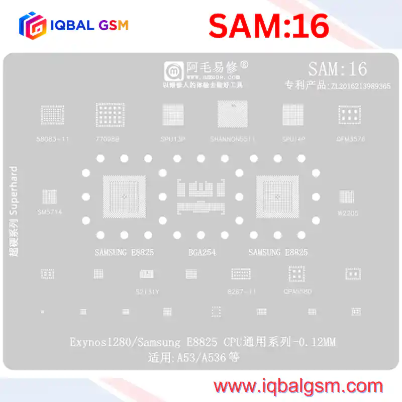
* Seat the cleaned CPU (SM6150, SDM660, SDM450, or MT6762) into its designated aperture on the AMAOE SAM:13 plate.
* Verify under stereo magnification (10x-20x) that all BGA pads align squarely with the laser openings.
* Squeeze Sn63/Pb37 paste onto lint-free paper and press firmly with a spatula to absorb excess flux solvent until the paste achieves a matte, putty-like consistency.
* Scrape paste firmly into the apertures with a stainless steel squeegee at a 45° angle. Scrape surface clean in a single diagonal stroke.
- Solder Ball Formation:
* Air Station Parameters: Temperature: 285°C - 300°C | Airflow: 25% - 30% (Low airflow prevents ball popping).
* Direct nozzle 3cm - 4cm above the plate. Warm the surrounding steel plate first to relieve thermal stress, then sweep smoothly across the aperture grid.
* Watch the paste melt into gleaming spherical balls. Allow 10 seconds to cool, then release the chip from the stencil underside using ESD tweezers.
- Secondary Ball Finishing:
* Apply a micro-droplet of liquid flux over the reballed spheres.
* Reflow with hot air at 280°C for 3 seconds to perfect sphericity and eliminate micro-burrs.
3. MOTHERBOARD SOLDERING & ALIGNMENT
- Dispense a micro-thin, uniform sheen of high-tack flux across the motherboard BGA pad array.
- Align the Pin 1 orientation index (laser dot on CPU corner) with the silkscreen bracket on the PCB.
- Soldering Parameters:
* Temperature: 330°C - 340°C | Airflow: 40% - 45%.
* Heat in smooth, wide circular loops around the chip boundary, gradually closing inward.
* Once the solder reflows, the chip will sink slightly and self-center. Give one corner a microscopic tap with fine tweezers (<0.2mm displacement); the IC will immediately bounce back into center position due to liquid solder surface tension.
- Allow the motherboard to cool naturally for 3 minutes before connecting DC power.
COLD DIODE-MODE & DC BENCH SUPPLY DIAGNOSTIC MATRIX
1. BENCH DC POWER SUPPLY CURRENT SIGNATURES (4.0V VPH_PWR / VBAT HOOKUP)
- Fault Signature 1: Direct Dead Short (0.000A -> Instant Over-Current Protection Trip @ 2.0A - 5.0A)
* Defect: Primary VPH_PWR or VBAT bus dead short to ground.
* Root Cause: High-side buck MOSFET breakdown inside PM6150 / PM660A (Qualcomm) or MT6357CRV (MediaTek), or shorted 22uF ceramic decoupling capacitor on VPH_PWR near the main coils.
* Action: Inject 1.2V / 3A on VPH_PWR with a thermal camera. If the PMIC glows instantly at 0V, replace the affected IC.
- Fault Signature 2: Total Zero Current Draw on Power Key Press (0.000A Static)
* Defect: Standby power domain non-functional or PWR_KEY_N circuit open.
* Root Cause: Broken trace on PWR_KEY_N line (missing 1.8V pull-up); dead 32.768 kHz RTC crystal; missing VDD_AO / VRTC standby rail; cracked solder ball under PMIC battery input pins.
- Fault Signature 3: Micro-Current Freeze (0.020A - 0.045A Constant Draw)
* Defect: PMIC initiates boot, but Reference Clock or digital core logic fails.
* Root Cause: Defective 19.200 MHz / 26.000 MHz reference crystal; short circuit on VDD_DIG / VCORE rail (0.80V - 0.85V); open circuit on I2C/SPMI communication bus between CPU and PMIC.
- Fault Signature 4: PC Communication Diagnostic Test
* Qualcomm Variant (Galaxy A70 / A60 / A9): Connect phone to PC via USB. If Device Manager enumerates "Qualcomm HS-USB QDLoader 9008" without test point shorting, all PMIC power rails are functional, but CPU cannot access RAM or eMMC/UFS flash storage. Reballing CPU and RAM is mandatory.
* MediaTek Variant (Galaxy A10s): Connect phone to PC via USB while holding Vol Down. If Device Manager detects "MediaTek USB Port (VCOM / Preloader)" (VID: 0E8D, PID: 0003), the MT6762 CPU, internal USB PHY, and MT6357CRV PMIC are 100% operational; fault is software crash or damaged eMMC storage.
- Fault Signature 5: Medium Current Bootloop (Hunts 0.080A -> 0.220A -> Drops to 0.000A -> Repeats)
* Defect: Missing PS_HOLD handshake from the Application Processor.
* Root Cause: PMIC generates all buck rails and asserts RESET_N, but processor crashes during bootloader execution due to corrupted eMMC/UFS storage, broken memory clock line, or cold solder joints under the memory chip.
2. COLD DIODE-MODE IMPEDANCE BENCHMARKS (RED PROBE TO GROUND, BLACK PROBE TO TARGET TEST POINT/INDUCTOR)
- Baseline Diode Readings for Qualcomm SM6150 / PM6150 (Galaxy A70):
* VPH_PWR Main Rail : 0.380V - 0.460V (If <0.100V: Primary system short)
* VDD_APC0 Core Buck (Inductor) : 0.065V - 0.120V (Low diode reading is normal for high-current core)
* VDD_APC1 Core Buck (Inductor) : 0.065V - 0.120V (If 0.000V: Silicon die shorted)
* VDD_MEM LPDDR4X Rail (Inductor) : 0.270V - 0.340V (If <0.110V: RAM die compromised)
* VDD_IO System 1.8V Rail (Inductor): 0.350V - 0.430V (If <0.180V: Peripheral bus shorted)
* VDD_DIG Baseband Core Buck : 0.220V - 0.300V (If <0.075V: Digital core leak)
* SPMI_CLK / SPMI_DATA Bus Lines : 0.410V - 0.480V (If OL: Broken ball under PMIC/CPU; if 0.000V: Bus shorted)
* PWR_KEY_N Power Key Line : 0.580V - 0.680V (If OL: Trace disconnect to PMIC)
* PS_HOLD Line : 0.420V - 0.500V (If 0.000V: CPU PS_HOLD pin shorted; if OL: Broken joint)
- Baseline Diode Readings for MediaTek MT6762 / MT6357CRV (Galaxy A10s):
* VBAT Battery Positive Connector : 0.420V - 0.500V (If <0.150V: Primary battery bus shorted)
* VPROC CPU Core Inductor : 0.160V - 0.240V (If 0.000V: MT6762 CPU core shorted)
* VCORE Digital Logic Inductor : 0.220V - 0.300V (If <0.080V: Internal logic leak)
* VIO18 System 1.8V Rail : 0.380V - 0.460V (If <0.180V: Peripheral bus shorted)
* 26.000 MHz Crystal Pins (OSC) : 0.550V - 0.640V (Must be balanced within 15mV)
* USB_DP / USB_DN Data Lines : 0.540V - 0.640V (Balanced within 10mV)