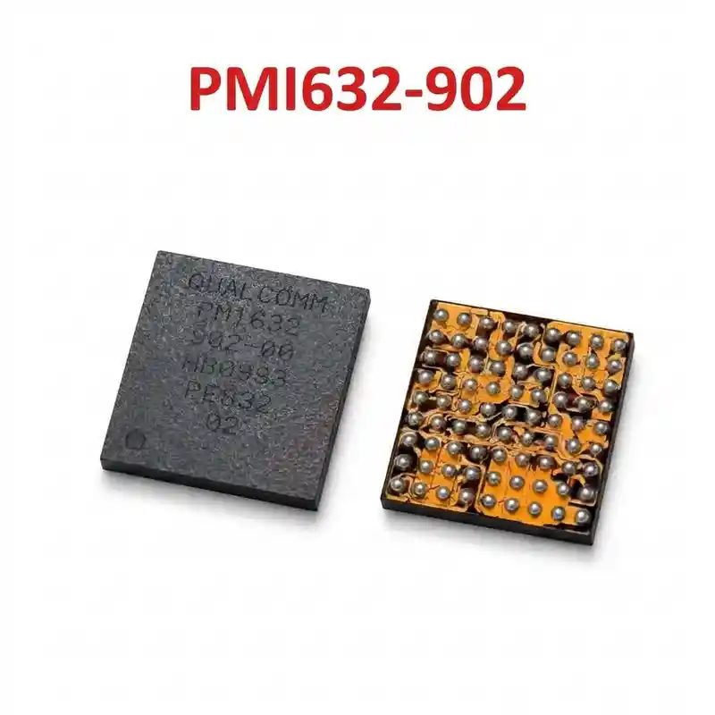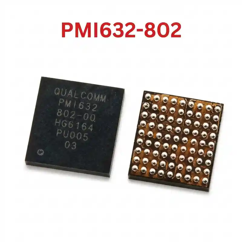

PMI632-602 IC
As low as
Rs 200.00
Worldwide shipping · Cash on Delivery
Product Details
====================================================================================================
QUALCOMM PMI632-602-00 SUB-PMIC / CHARGING & LIGHT IC REPAIR GUIDE
====================================================================================================
1. PRODUCT IDENTIFICATION & SILICON SPECIFICATIONS:
----------------------------------------------------------------------------------------------------
- Silicon Laser Marking: PMI632 [Line 2: 602-00 or 602]
- Commercial Hardware Name: Qualcomm Secondary Intermediate Power Management Subsystem
- Silicon Manufacturer: Qualcomm Technologies, Inc.
- System Classification: Secondary Power Management IC (Sub-PMIC / Charger / Light Driver)
- Associated Main Platforms: Qualcomm Snapdragon 439, 450, 632 platforms
- Companion Primary PMIC: Qualcomm PM439 / PM8953 (board dependent)
- Package Form Factor: Fine-Pitch 72-Pin BGA (BGA72 / WLCSP)
- Key Internal Functional Blocks:
* Switch-Mode Battery Charger:
- Supports programmable input current limit (up to 3.0A) and battery CV/CC profiles.
* Primary Bus Power Generator (VPH_PWR):
- Regulates system rail (3.7V – 4.2V DC) distributed to Main PMIC, PA, and peripherals.
* High-Voltage WLED Backlight Driver:
- Step-up DC-DC boost converter generating 18V – 25V DC with multi-string cathode sinks.
* Camera Flash LED Driver:
- Dual/single output high-current flash driver with strobe trigger.
* Fuel Gauge & Battery Sensing:
- Precise ADC tracking battery impedance, open-circuit voltage, and NTC thermal lines.
* USB OTG 5V Output:
- 5V step-up booster delivering 500mA–1A for connected USB peripherals.
2. COMPATIBLE SMARTPHONES & REVISION SPECIFICITY:
----------------------------------------------------------------------------------------------------
- Primary Target Device Platform:
* Vivo Y95 (Snapdragon 439 - Model 1807)
* Vivo Y93 / Vivo Y91 (Snapdragon editions)
* Vivo Y73 (Qualcomm edition)
- Secondary Compatibility:
* Oppo A5 / Oppo A7 (specific board revisions)
*(Crucial Note: Replacing 602 with 502 or 902 on Vivo Y95 logic boards frequently triggers no backlight,
dimming inverted curves, or boot-looping at the Vivo logo due to factory OTP register mismatch)*
3. TYPICAL BOARD-LEVEL FAULT SYMPTOMS:
----------------------------------------------------------------------------------------------------
- Dead Device / Complete Power Failure (0.00A – 0.02A Consumption on DC Bench Supply):
* Failure of internal buck circuit stops VPH_PWR generation. Main PMIC and CPU receive no power.
- Fake Charging / 0.00A–0.10A Current Draw on USB Meter:
* Phone detects charging cable (battery icon appears) but fails to pass current; battery continuously drains.
- Display Backlight Outage (Black Screen, Board Fully Alive):
* Handset vibrates on boot, rings on incoming calls, and shows faint graphics under strong lamp,
but screen illumination remains pitch black (blown boost diode, inductor, or internal 602 driver).
- Vivo Logo Boot Loop or "Battery Temperature Too Low" Error:
* Corrupted battery thermistor ADC lines inside PMI632 halt the boot process at first vendor splash.
- VPH_PWR / Battery Rail Short to Ground:
* Punctured high-side MOSFET clamps the main system power rail directly to GND (0.000V in diode mode).
4. STEP-BY-STEP MULTIMETER TESTING & DIAGNOSTICS:
----------------------------------------------------------------------------------------------------
A. Cold Testing (Diode Mode Check - Board Powered Off, Battery Disconnected):
1. Connect Multimeter RED probe to Motherboard Ground (GND), probe test points with BLACK probe:
- VBUS Input Filter Capacitor (adjacent to USB charging line): Normal ~450mV – 550mV.
- Battery Connector Positive Pin (VBAT): Normal ~400mV – 480mV.
- VPH_PWR Inductor (large coil directly beside PMI632): Normal ~350mV – 450mV (0.000V = dead short).
- Backlight Anode Line / Boost Diode Cathode: Normal ~420mV – 520mV.
- Boot Capacitor (BST): Probe across the two ends of the capacitor; must show high impedance (no short).
2. Short-Circuit Isolation:
- If VPH_PWR reads 0.000V, inject 3.7V DC (limited to 2.0A) onto the inductor.
Inspect with thermal camera: if PMI632 lights up brightly, desolder the IC.
B. Live Operating Voltage Check (Hot Testing):
1. Insert 5V USB charger cable into the phone:
- VBUS capacitor: Must show 5.0V – 5.2V DC steady.
- VPH_PWR Inductor: Must output steady 3.7V – 4.2V DC (even with battery detached).
- Battery terminal pins: Must show pulsating 3.7V – 4.35V DC charging voltage.
2. Trigger board power-on:
- Backlight Anode terminal: Must read 3.7V in standby, then jump to 18V – 25V DC once the display
driver wakes up. If it remains stuck at battery voltage (3.7V), replace PMI632-602-00.
5. SOLDERING, REBALLING & REWORK SPECIFICATIONS:
----------------------------------------------------------------------------------------------------
- Surrounding Component Thermal Protection:
* PMI632 is positioned under a solder-down metal shield near the eMMC/UFS memory and CPU.
* Always protect adjacent memory and processor chips with Kapton thermal tape and copper coins.
- IC Removal:
* Dispense high-grade non-corrosive RMA BGA tacky flux around the chip.
* Hot air rework station settings: 320°C – 335°C, airflow 35% – 45% (medium nozzle).
* Circle nozzle uniformly for 30–40 seconds. Once all solder joints liquefy, lift chip vertically.
- PCB Pad Preparation:
* Apply 183°C leaded solder (Sn63/Pb37) to logic board footprint to dilute high-melt unleaded alloy.
* Flatten pad matrix using copper desoldering braid with soldering iron set to 290°C – 300°C.
* Clean thoroughly with 99% Isopropyl Alcohol (IPA); check pads under microscope for any damage.
- Reballing Procedure:
* Use a dedicated or universal 0.12mm BGA stencil matching the 72-pin PMI632 footprint.
* Spread 183°C solder paste smoothly across all apertures with a metal scraper.
* Reflow gently at 280°C with 20% airflow until uniform solder spheres emerge.
- Placement & Alignment:
* Spread a thin, transparent layer of tacky BGA flux onto PCB pads.
* Align Pin 1 dot on the PMI632 chip with silkscreen corner indicator.
* Reflow at 310°C – 320°C with 35% airflow; observe the chip pull into place by solder surface tension.
* Allow motherboard to cool naturally for 3–5 minutes before connecting DC power or battery.
====================================================================================================
You may also like