PM8998 IC
As low as
Rs 0.00
Worldwide shipping · Cash on Delivery
Product Details
====================================================================================================
QUALCOMM PM8998 / PM8998-002 SNAPDRAGON 835 MASTER CORE PMIC REPAIR GUIDE
====================================================================================================
1. PRODUCT IDENTIFICATION & SILICON SPECIFICATIONS:
----------------------------------------------------------------------------------------------------
- Silicon Laser Marking: PM8998 (Common Production Variant: PM8998-002 / PM8998 002)
- Silicon Manufacturer: Qualcomm Technologies, Inc.
- Semiconductor Process Node: Samsung 10nm LPE (Low Power Early) FinFET Architecture
- System Classification: Primary Master Core Power Management IC (Core PMIC & Voltage Orchestrator)
- Associated SoC Platforms: Qualcomm Snapdragon 835 (MSM8998 Octa-Core 2.45GHz)
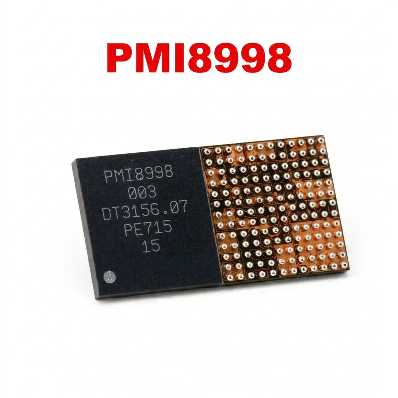
- Multi-PMIC Triad Architecture: PM8998 (Master Core & LDOs) + PMI8998 (Charger/VPH_PWR/AMOLED/Flash)
- Package Form Factor: Fine-Pitch Wafer-Level Chip-Scale BGA (WLCSP)
- Regulated Output Domains:
* Multi-Phase Synchronous Step-Down Buck Converters:
- VDD_APC0 (Kryo 280 Silver Efficiency Cluster up to 1.9GHz): 0.65V – 1.05V Dynamic Voltage Scaling.
- VDD_APC1 (Kryo 280 Gold Performance Cluster up to 2.45GHz): 0.65V – 1.15V DVS.
- VDD_GPU (Adreno 540 Graphics Processing Unit Core): 0.65V – 1.05V DVS.
- VDD_MEM / VDD_DDR (Dual-Channel LPDDR4X Memory Rails): Clean 1.10V / 0.60V VDDQ.
- VDD_MODEM (Snapdragon X16 Gigabit LTE Baseband Core): 0.85V – 1.05V.
* 30+ Precision Ultra-Low Noise Linear (LDO) Regulators:
- Dedicated clean supplies for UFS 2.1 storage (2.95V VCC, 1.8V VCCQ, 1.2V VCCQ2).
- Multi-channel Camera Sensor rails (AVDD 2.8V, DVDD 1.1V, OIS 3.0V).
- Display interface, touch digitizer, and high-speed PCIe peripheral power lines.
* Clocks & System Reset Management:
- Integrated 19.2MHz system reference clock crystal (XO) oscillator driver circuit.
- Hardware Power-Key debounce logic (KYPD_PWR_N).
- Master cold-boot reset tree generator (PON_RESET_N) with continuous PS_HOLD (1.8V) verification.
2. COMPATIBLE 4G FLAGSHIP SMARTPHONES:
----------------------------------------------------------------------------------------------------
- Samsung Galaxy:
* Galaxy S8 (SM-G950U, SM-G950W, SM-G9500)
* Galaxy S8+ / S8 Plus (SM-G955U, SM-G955W, SM-G9550)
* Galaxy Note 8 (SM-N950U, SM-N950W, SM-N9500)
* Galaxy S8 Active (SM-G892A)
- Xiaomi:
* Xiaomi Mi 6 (Sagit)
* Xiaomi Mi MIX 2 (Chiron)
- OnePlus:
* OnePlus 5 (A5000), OnePlus 5T (A5010)
- Google Pixel:
* Google Pixel 2 (Walleye), Google Pixel 2 XL (Taimen)
- Sony Xperia:
* Xperia XZ Premium (G8141, G8142)
* Xperia XZ1 (G8341, G8342), Xperia XZ1 Compact (G8441)
- LG, HTC & Others:
* LG V30 / V30+ (H930, H932, US998)
* HTC U11 / HTC U11+, Nokia 8 (TA-1004, TA-1012), Essential Phone PH-1
3. TYPICAL BOARD-LEVEL FAULT SYMPTOMS:
----------------------------------------------------------------------------------------------------
- Completely Dead Logic Board (0.000A Current on Power Key Trigger):
* Bench power supply shows 0.000A upon pressing the power button.
* Cause: Internal power key contact pull-up resistor blown, shorted 1.8V LDO rail, or defective 19.2MHz
crystal oscillator circuit inside PM8998.
- Low Current Boot Freeze / Hang on Logo (0.06A – 0.12A Freeze):
* Current jumps to ~80mA–110mA and hangs permanently on DC supply without pulsating.
* Cause: Missing Kryo 280 core buck voltages (VDD_APC0/APC1) or missing UFS 2.1 storage power rails.
- Instant Drop to Zero Current on Power Key Release:
* DC power supply current jumps to 80mA–120mA while holding the power switch, but instantly collapses
back to 0.00A as soon as the button is released.
* Cause: Missing PS_HOLD handshake (1.8V) from MSM8998 CPU, or unacknowledged PON_RESET_N signal.
- Emergency Qualcomm HS-USB QDLoader 9008 Port Detection:
* Device remains on a black screen and connects directly to PC as 9008 COM port due to missing or
unstable UFS 2.1 storage power lines (2.95V / 1.8V / 1.2V).
- Primary System Power Rail Breakdown:
* Breakdown of internal high-side buck MOSFET shorts an internal core rail directly to ground,
causing high current draw and severe heating around PM8998.
4. STEP-BY-STEP MULTIMETER TESTING & DIAGNOSTICS:
----------------------------------------------------------------------------------------------------
A. Cold Testing (Diode Mode Check - Board Powered Off, Battery Disconnected):
1. Place digital multimeter in Diode Mode. Connect RED probe to motherboard GND shield:
- Main VPH_PWR / VSYS Rail: Normal ~370mV – 470mV.
- VDD_APC0 (Efficiency Core Inductors): Normal ~40mV – 75mV.
- VDD_APC1 (Gold Performance Core Inductors): Normal ~30mV – 65mV (low resistance, must NOT be 0.000V).
- VDD_GPU (Adreno 540 Inductor): Normal ~25mV – 60mV.
- VREG_L5_1P8 (1.8V System IO Rail): Normal ~360mV – 470mV.
- UFS Storage VCC 2.95V Output Capacitor: Normal ~420mV – 540mV.
- Power Key Contact Point: Normal ~500mV – 650mV.
2. Short-Circuit Isolation:
- If an internal buck rail reads 0.000V (beeping dead short to ground), inject 1.0V DC (current limit 2.0A).
Observe PM8998 with thermal camera or rosin vapor; if it glows white-hot, remove the IC.
B. Live Operating Voltage Check (Hot Testing):
1. Connect DC power supply at 3.8V to battery connector terminals:
- Check Power Key terminal: Must measure steady 1.8V DC.
2. Press and hold Power Button while probing output coils:
- VDD_APC0 core coil must measure 0.85V – 1.05V DC.
- VDD_APC1 core coil must measure 0.90V – 1.15V DC.
- Verify 1.8V and 2.95V at UFS storage bypass capacitors.
- Check PS_HOLD test point: Must rise from 0V to 1.8V and stay locked high. If PS_HOLD drops back
to 0V within 1–2 seconds, CPU/UFS communication has failed.
5. SOLDERING, REBALLING & REWORK SPECIFICATIONS:
----------------------------------------------------------------------------------------------------
- Thermal Shielding (10nm Multi-Layer PCB Sensitivity):
* PM8998 sits in close proximity to the 10nm Snapdragon 835 CPU/UFS stack and companion PMI8998 PMIC.
* Always shield the neighboring CPU, UFS storage, and PMI8998 with multi-layer Kapton heat tape and copper heat sinks.
- IC Removal:
* Dispense high-grade, non-corrosive RMA tacky BGA flux around the perimeter of PM8998.
* Hot air rework station settings: 315°C – 325°C with 40% – 45% airflow (medium circular nozzle).
* Apply heat uniformly in circles for 35–50 seconds. Once all solder balls liquefy, lift the IC vertically.
- PCB Pad Cleanup:
* Apply leaded solder (Sn63/Pb37) to motherboard footprint pads to lower the melting threshold.
* Level pads perfectly flat using copper desoldering braid and a soldering iron tip set to 290°C – 300°C.
* Clean residual flux thoroughly with 99% Isopropyl Alcohol (IPA); inspect pads under microscope.
- Reballing Procedure:
* Use a 0.12mm dedicated Amaoe PM2 or Snapdragon 835 PM8998 BGA stencil.
* Squeegee 183°C leaded solder paste uniformly into all stencil apertures.
* Reflow gently with hot air at 280°C – 290°C with low airflow (20%) until uniform solder spheres form.
- Alignment & Installation:
* Spread a microscopic, transparent film of BGA flux over PCB pads.
* Align Pin 1 orientation dot precisely with the PCB silkscreen corner indicator.
* Reflow at 305°C – 315°C with 35% airflow until chip self-centers on solder surface tension.
* Allow motherboard to cool naturally to room temperature for 5 minutes before connecting DC power.
====================================================================================================