PM8953 IC
As low as
Rs 0.00
Worldwide shipping · Cash on Delivery
Product Details
====================================================================================================
QUALCOMM PM8953 / PM8953-0VV SNAPDRAGON 625/450 PRIMARY PMIC REPAIR GUIDE
====================================================================================================
1. PRODUCT IDENTIFICATION & SILICON SPECIFICATIONS:
----------------------------------------------------------------------------------------------------
- Silicon Laser Marking: PM8953 (Common Production Variant: PM8953-0VV / PM8953 0VV)
- Silicon Manufacturer: Qualcomm Technologies, Inc.
- Semiconductor Process Node: 14nm FinFET Architecture (Optimized Low-Power Power Management)
- System Classification: Primary Master Core PMIC (Core Processor Power & System Sequencing)
- Associated SoC Platforms: Qualcomm Snapdragon 625 (MSM8953), Snapdragon 626 (MSM8953 Pro), Snapdragon 450 (SDM450)
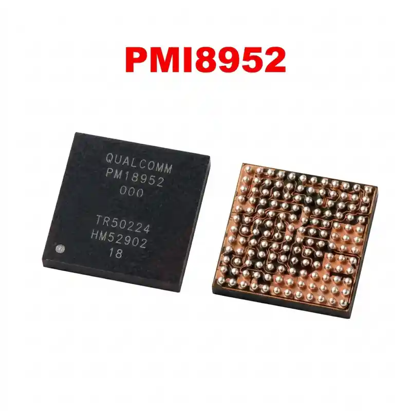
- Multi-PMIC Architecture: PM8953 (Primary Master) + PMI8952 (Secondary Charger/Backlight/Flash/Display Bias)
- Package Form Factor: 183-Pin Fine-Pitch Wafer-Level Chip-Scale BGA (WLCSP)
- Regulated Output Domains:
* Multi-Phase Synchronous Step-Down Buck Regulators:
- VDD_APC0 (Cortex-A53 Efficiency Cluster): 0.70V – 1.15V Dynamic Voltage Scaling (DVS).
- VDD_APC1 (Cortex-A53 Performance Cluster up to 2.0GHz): 0.70V – 1.25V DVS.
- VDD_MSS (Modem Baseband Core & Hexagon 546 DSP): 0.95V – 1.15V.
- VDD_MEM / VDD_DDR (LPDDR3 High-Speed Memory Rails): Clean 1.225V / 1.80V.
* 25+ Precision Ultra-Low Noise Linear (LDO) Regulators:
- VREG_L5_1P8 (1.8V System IO, Peripheral Sensors, and eMMC VCCQ).
- VREG_L11_2P95 (2.95V eMMC 5.1 Flash Memory Core VCC).
- VREG_L17_2P85 (2.85V Display MIPI Interface & Camera Sensor Analog).
- Clean analog power rails for WTR2965 / WTR3925 RF Transceivers, GPS, and Wi-Fi/BT.
* Clocks & System Reset Management:
- Integrated 19.2MHz system reference clock crystal (XO) oscillator driver circuit.
- Hardware Power-Key debounce circuitry (KYPD_PWR_N).
- Master cold-boot reset tree generator (PON_RESET_N) with continuous PS_HOLD (1.8V) verification.
2. COMPATIBLE SMARTPHONES & DEVICES:
----------------------------------------------------------------------------------------------------
- Xiaomi:
* Redmi Note 4 / Redmi Note 4X (Qualcomm Snapdragon "Mido")
* Xiaomi Mi A1 / Xiaomi Mi 5X
* Xiaomi Redmi 6 Pro
* Xiaomi Mi Max 2
- Samsung Galaxy:
* Galaxy J8 2018 (SM-J810F, SM-J810G, SM-J810Y)
* Galaxy A6+ / A6 Plus (SM-A605F, SM-A605G)
* Galaxy A11 (SM-A115F, SM-A115M)
* Galaxy A02s / Galaxy M02s (SM-A025F, SM-M025F)
* Galaxy C7 / C7 Pro (SM-C7000, SM-C7010)
* Galaxy Tab A 10.5 2018 (SM-T590, SM-T595)
- Motorola:
* Moto G5 Plus (XT1684, XT1685, XT1687)
* Moto G5S Plus (XT1802, XT1804, XT1805)
- Vivo & Oppo:
* Vivo V7 / V7 Plus (1716, 1718), Vivo V9 (SD626 / SD450 editions)
* Oppo A73, Oppo A71 2018
3. TYPICAL BOARD-LEVEL FAULT SYMPTOMS:
----------------------------------------------------------------------------------------------------
- Completely Dead Handset (0.000A DC Bench Power Supply Draw):
* Connecting DC power supply to battery terminals and pressing the power button draws strictly 0.000A.
* Cause: Internal power key contact pull-up resistor blown, shorted 1.8V LDO rail, or defective 19.2MHz
crystal oscillator circuit inside PM8953.
- Low Current Boot Freeze / Hang on Logo (0.05A – 0.08A Freeze):
* When pressing power button, current rises to ~50mA–80mA and hangs permanently without pulsating.
* Cause: Missing Cortex-A53 core buck voltages (VDD_APC0/APC1) or missing eMMC storage power (2.95V VCC).
- Instant Drop to Zero Current on Power Key Release:
* DC power supply current jumps to 60mA–100mA while holding the power switch, but instantly collapses
back to 0.00A as soon as the button is released.
* Cause: Missing PS_HOLD handshake (1.8V) from CPU, or unacknowledged PON_RESET_N signal.
- Emergency Qualcomm HS-USB QDLoader 9008 Port Detection:
* Handset screen remains completely black, but device connects to PC in 9008 emergency download mode
due to corrupted eMMC power supply rails generated by PM8953.
- Primary VPH_PWR / VSYS Line Short Circuit:
* Breakdown of internal high-side buck MOSFET shorts the main 4.0V system line directly to ground,
causing high current draw (1.5A - 2.5A) and severe heating around PM8953.
4. STEP-BY-STEP MULTIMETER TESTING & DIAGNOSTICS:
----------------------------------------------------------------------------------------------------
A. Cold Testing (Diode Mode Check - Board Powered Off, Battery Disconnected):
1. Place digital multimeter in Diode Mode. Connect RED probe to motherboard GND shield:
- Main VPH_PWR / VSYS Rail: Normal ~380mV – 480mV.
- VDD_APC0 / APC1 (CPU Core Inductors): Normal ~50mV – 90mV (low resistance, must NOT be 0.000V).
- VDD_MSS (Modem Buck Coil): Normal ~100mV – 165mV.
- VREG_L5_1P8 (1.8V System IO Rail): Normal ~360mV – 470mV.
- eMMC VCC 2.95V Output Capacitor: Normal ~420mV – 540mV.
- Power Key Contact Point: Normal ~500mV – 650mV.
2. Short-Circuit Isolation:
- If VPH_PWR reads 0.000V (beeping continuity to ground), inject 3.7V DC (current limit 1.5A).
Check PM8953 and surrounding MLCC bypass capacitors with thermal camera or rosin vapor.
B. Live Operating Voltage Check (Hot Testing):
1. Connect DC power supply at 3.8V to battery connector terminals:
- Check Power Key terminal: Must measure steady 1.8V DC.
2. Press and hold Power Button while probing output coils:
- VDD_APC0 and APC1 core buck coils must measure 0.90V – 1.15V DC.
- VDD_MSS modem buck coil must measure steady 1.05V DC.
- Verify 1.8V and 2.95V at eMMC bypass capacitors.
- Check PS_HOLD test point: Must rise from 0V to 1.8V and stay locked high. If PS_HOLD drops back
to 0V within 1–2 seconds, CPU/eMMC communication has failed.
5. SOLDERING, REBALLING & REWORK SPECIFICATIONS:
----------------------------------------------------------------------------------------------------
- Thermal Shielding:
* PM8953 is situated in close proximity to the Snapdragon 625 CPU and eMMC storage stack.
* Always shield the neighboring CPU, eMMC, and secondary PMI8952 with multi-layer Kapton tape and thick copper coins.
- IC Removal:
* Dispense high-grade, non-corrosive RMA tacky BGA flux around PM8953.
* Hot air rework station settings: 315°C – 325°C with 40% – 45% airflow (standard circular nozzle).
* Heat evenly in circles for 35–50 seconds. Once all 183 solder balls liquefy, lift the IC vertically.
- PCB Pad Cleanup:
* Apply leaded solder (Sn63/Pb37) to motherboard footprint pads to lower the melting threshold.
* Level pads perfectly flat using copper desoldering braid and a soldering iron tip set to 290°C – 300°C.
* Clean residual flux thoroughly with 99% Isopropyl Alcohol (IPA); inspect pads under microscope.
- Reballing Procedure:
* Use a 0.12mm dedicated Amaoe PM1 or Amaoe PM2 Qualcomm PMIC stencil.
* Squeegee 183°C leaded solder paste uniformly into all stencil apertures.
* Reflow gently with hot air at 280°C – 290°C with low airflow (20%) until uniform solder spheres form.
- Alignment & Installation:
* Spread a microscopic, transparent film of BGA flux over PCB pads.
* Align Pin 1 orientation dot precisely with the PCB silkscreen corner indicator.
* Reflow at 305°C – 315°C with 35% airflow until chip self-centers on solder surface tension.
* Allow motherboard to cool naturally to room temperature for 5 minutes before connecting DC power.
====================================================================================================