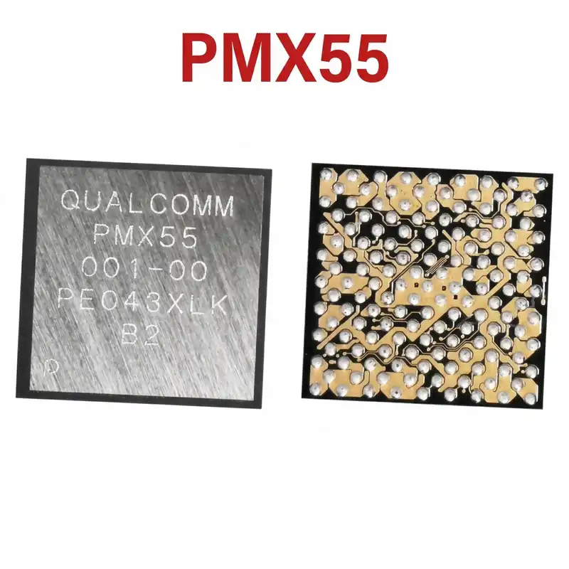
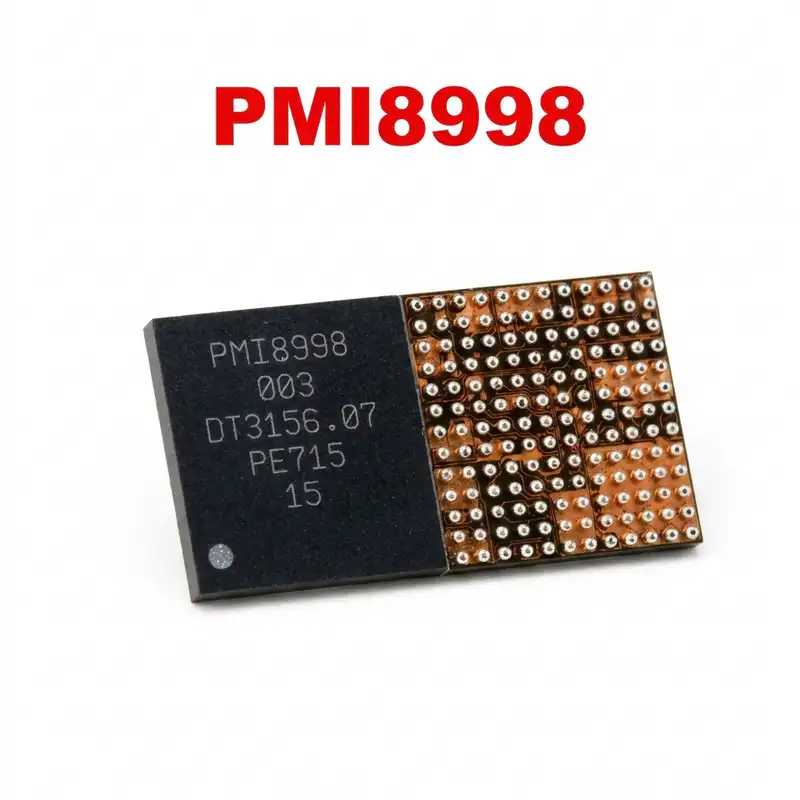
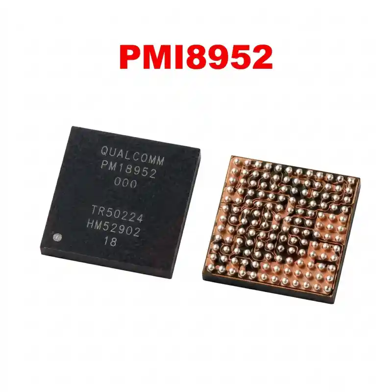
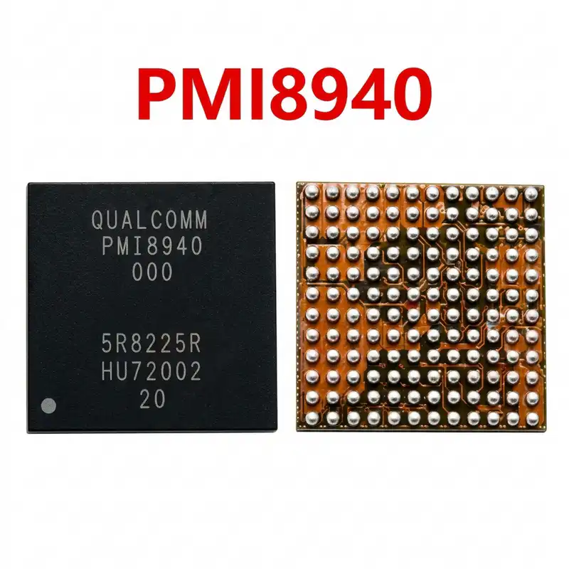
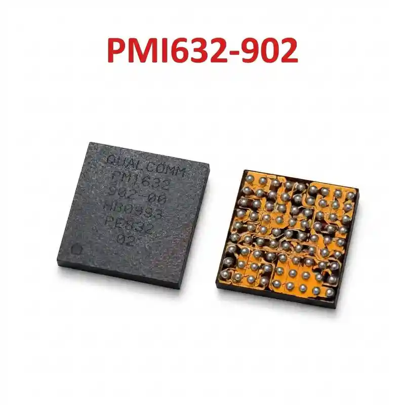
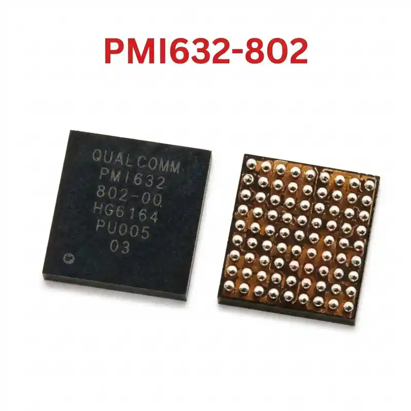
PM8909 IC
As low as
Rs 180.00
Worldwide shipping · Cash on Delivery
Product Details
====================================================================================================
QUALCOMM PM8909 / PM8909-002 ALL-IN-ONE PRIMARY PMIC REPAIR GUIDE
====================================================================================================
1. PRODUCT IDENTIFICATION & SILICON SPECIFICATIONS:
----------------------------------------------------------------------------------------------------
- Silicon Laser Marking: PM8909 (Common Variant Code: PM8909-002 / PM8909 002)
- Silicon Manufacturer: Qualcomm Technologies, Inc.
- System Classification: All-in-One Integrated Power Management Unit (PMIC + Charger + Codec)
- Associated SoC Platforms: Qualcomm Snapdragon 210 (MSM8909), Snapdragon 212 (APQ8009 / SDM205)
- Architecture Type: Single-Chip High-Integration PMU (Monolithic Power + Analog Hub)
- Package Form Factor: Wafer-Level Chip-Scale BGA (WLCSP)
- Regulated Output Domains:
* Synchronous Step-Down Buck Converters:
- VDD_MSS (Modem Subsystem Digital Core): 0.95V – 1.15V.
- VDD_APC (Quad-Core Cortex-A7 Application Processor Cluster): 0.90V – 1.25V Dynamic Scaling.
- VDD_MEM / VDD_DDR (LPDDR2/3 Memory Rails): Clean 1.20V / 1.80V.
* 20+ Low-Dropout Linear Regulators (LDOs):
- VREG_L6_1P8 (1.8V System IO & eMMC VCCQ).
- VREG_L11_2P95 (2.95V eMMC Flash Storage Core VCC).
- VREG_L17_2P85 (2.85V Display & Touch Screen Power).
- Low-noise dedicated rails for RF Front-End (WTR2965 / WTR4905 transceiver supplies).
* Integrated Charging & Analog Functions:
- Linear/Switch-mode 1.5A USB Battery Charger with Automatic Power-Path management.
- Power-on Reset Controller (PON_RESET_N) and 19.2MHz system clock generator circuit.
- Integrated Mono Class-D / AB Speaker Amplifier and Stereo Headphone Audio DAC.
2. COMPATIBLE 4G ENTRY-LEVEL SMARTPHONES & DEVICES:
----------------------------------------------------------------------------------------------------
- Samsung:
* Galaxy J1 4G (SM-J120F, SM-J120H, SM-J120M)
* Galaxy J2 2016 (Snapdragon variants)
* Galaxy Core Prime 4G (SM-G360V, SM-G361F)
* Galaxy Folder 2 Flip (SM-G1600)
- Nokia & HMD Global:
* Nokia 2 (TA-1029, TA-1035, TA-1007, TA-1011)
* Nokia 8110 4G (Smart Feature Phone)
- Huawei & Honor:
* Huawei Y6 4G (SCL-L01, SCL-L21, SCC-U21)
* Honor 4A (SCL-AL00, SCL-CL00)
- HTC & ZTE & Alcatel:
* HTC Desire 626s (A32EWHL), Desire 626N (A32EUL), Desire 520
* ZTE Blade A310, ZTE Avid Plus
* Alcatel One Touch Pixi 4 (5), Alcatel Pop 4
- Others:
* Wiko Rainbow Lite 4G, Wiko Tommy, itel / Tecno budget 4G smartphones, Quectel SC20 Smart Modules
3. TYPICAL BOARD-LEVEL FAULT SYMPTOMS:
----------------------------------------------------------------------------------------------------
- Dead Handset / Zero Current on DC Power Supply (0.000A):
* Pressing the power key registers no current draw at all on the DC power supply meter.
* Cause: Defective internal power-key debounce circuit (PWR_KEY_N), shorted VREG_L6_1P8 rail, or failed
19.2MHz crystal oscillator driver.
- Stuck Low Current Boot Hang (0.04A – 0.08A Freeze):
* When pressing power button, current rises to ~50mA–70mA and remains frozen without boot pulsation.
* Cause: Missing Cortex-A7 core voltage (VDD_APC) or missing eMMC storage power (2.95V VCC / 1.8V VCCQ).
- Emergency 9008 Mode or Dead After Flashing:
* Phone connects to PC strictly as "Qualcomm HS-USB QDLoader 9008" with no screen illumination.
* Cause: Unstable storage power delivery or missing reset acknowledgment line (PS_HOLD failure).
- Fake Charging or No Battery Current (0.00A / Plugged in but Discharging):
* Charging icon appears on LCD, but battery current is 0.00A on USB meter due to burned internal charging
switching FETs or cracked solder joints beneath the VBUS input pins.
- No Sound / Audio Distortion (Earpiece & Speaker Dead):
* Because PM8909 houses the internal audio codec, water ingress near this IC frequently destroys audio
output paths while the phone still powers on normally.
4. STEP-BY-STEP MULTIMETER TESTING & DIAGNOSTICS:
----------------------------------------------------------------------------------------------------
A. Cold Testing (Diode Mode Check - Board Powered Off, Battery Disconnected):
1. Place multimeter in Diode Mode. Connect RED probe to motherboard GND shield:
- Main VSYS / VBAT Positive Rail: Normal ~380mV – 490mV.
- VDD_APC (CPU Core Inductor): Normal ~80mV – 140mV (ultra-low resistance, but never 0.000V).
- VDD_MSS (Modem Buck Inductor): Normal ~120mV – 190mV.
- VREG_L6_1P8 (1.8V System IO Capacitor): Normal ~350mV – 460mV.
- eMMC VCC 2.95V Capacitor: Normal ~420mV – 540mV.
- Power Key Contact Point: Normal ~500mV – 650mV.
2. Short-Circuit Detection:
- If VBAT/VSYS shows 0.000V (beeping continuity to ground), apply 3.7V DC (1.5A limit). Check PM8909
and surrounding bypass MLCC capacitors using rosin vapor or thermal imaging.
B. Live Operating Voltage Check (Hot Testing):
1. Connect DC bench power supply set to 3.8V to battery pins:
- Check Power Key terminal: Must measure steady 1.8V DC.
2. Press and hold Power Button:
- VDD_APC core coil must rise to 1.05V – 1.15V DC.
- VDD_MSS coil must measure 1.0V DC.
- Check eMMC capacitors: Steady 1.8V and 2.95V must be present.
- Check PS_HOLD test point: Must rise from 0V to 1.8V and stay locked high. If PS_HOLD drops back
to 0V within 1–2 seconds, CPU/eMMC communication is interrupted.
5. SOLDERING, REBALLING & REWORK SPECIFICATIONS:
----------------------------------------------------------------------------------------------------
- IC Removal:
* Apply mild, non-corrosive RMA tacky BGA soldering flux around PM8909.
* Hot air rework station settings: 310°C – 320°C with 40% airflow (standard circular nozzle).
* Heat evenly in circles for 30–45 seconds. As solder balls melt completely, lift vertically with tweezers.
- PCB Pad Cleanup:
* Apply 183°C leaded solder to motherboard pads to lower the eutectic threshold.
* Level pads using high-grade copper desoldering wick and a hoof/knife soldering tip at 290°C.
* Clean residual flux thoroughly with 99% Isopropyl Alcohol (IPA); verify pads under stereomicroscope.
- Reballing Procedure:
* Use a dedicated 0.12mm Amaoe PM1 or universal Qualcomm PMIC stencil.
* Apply 183°C (Sn63/Pb37) leaded solder paste evenly across all apertures.
* Heat gently at 280°C – 290°C with low airflow (20%) to form uniform solder spheres.
- Alignment & Reflow:
* Spread a microscopic film of flux over the board pads.
* Align Pin 1 dot precisely with the PCB silkscreen orientation corner.
* Reflow at 305°C – 315°C with 35% airflow. Tap lightly with tweezers to confirm self-alignment.
* Allow motherboard to cool completely before applying power.
====================================================================================================
You may also like