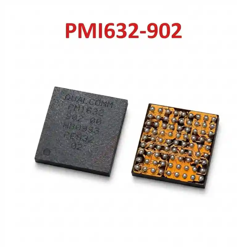
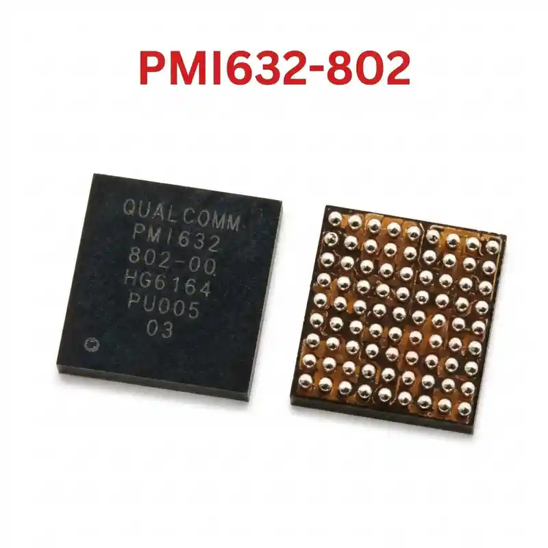
PM8350BHS IC
As low as
Rs 200.00
Worldwide shipping · Cash on Delivery
Product Details
====================================================================================================
QUALCOMM PM8350BHS / PM8350BHS-001 SECONDARY CHARGER & POWER MANAGEMENT IC GUIDE
====================================================================================================
1. PRODUCT IDENTIFICATION & SILICON SPECIFICATIONS:
----------------------------------------------------------------------------------------------------
- Silicon Laser Marking: PM8350BHS (Variant Code: PM8350BHS-001 / PM8350BHS 001)
- Silicon Manufacturer: Qualcomm Technologies, Inc.
- Semiconductor Process Node: Samsung 5nm EUV Advanced FinFET Architecture
- System Classification: Secondary PMIC, Switching Battery Charger, VPH_PWR & Flash LED Driver
- Associated SoC Platforms: Qualcomm Snapdragon 888 5G (SM8350), Snapdragon 888+ 5G (SM8350-AC)
- Multi-PMIC Triad Architecture: PM8350-004 (Master Core) + PM8350C (GPU/Display) + PM8350BHS (Charging/VPH)
- Package Form Factor: Fine-Pitch Wafer-Level Chip-Scale BGA (WLCSP)
- Functional Circuit Domains:
* Switch-Mode Battery Charger (SMBB):
- Supports Qualcomm Quick Charge 4+ / Quick Charge 5 & USB-PD PPS negotiation.
- Synchronous step-down buck conversion from USB VBUS (5V/9V/12V) down to battery charge voltage.
- Integrated Power-Path control: Dynamic arbitration between USB input, battery cell, and system load.
* System Voltage Generation (VPH_PWR):
- Supplies system base operating rail VPH_PWR / VSYS (3.6V – 4.2V) feeding all primary buck converters.
* Camera Flash LED Driver Subsystem:
- High-efficiency boost converter driving dual LED emitters up to 2.5A pulse current.
* Precision Analog & Thermal Monitoring:
- Battery temperature thermistor sensing (BATT_THERM) and internal die thermal shutdown loop.
- Reverse boost capability for USB OTG (5.0V output at Type-C connector).
* Peripheral Low-Noise Regulators:
- Secondary low-dropout (LDO) rails supporting RF front-end, audio codecs, and tactile vibration drivers.
2. COMPATIBLE 5G FLAGSHIP SMARTPHONES:
----------------------------------------------------------------------------------------------------
- Samsung (Qualcomm Snapdragon 888 Models):
* Galaxy S21 5G (SM-G991U), Galaxy S21+ 5G (SM-G996U), Galaxy S21 Ultra 5G (SM-G998U)
* Galaxy S21 FE 5G (SM-G990U / SM-G990U1)
* Galaxy Z Fold 3 5G (SM-F926U), Galaxy Z Flip 3 5G (SM-F711U)
- Xiaomi:
* Xiaomi Mi 11, Mi 11 Pro, Mi 11 Ultra, Mi 11i, Xiaomi 11 Lite 5G
* Mi MIX 4, Mi MIX FOLD
* Redmi K40 Pro / Redmi K40 Pro+
- OnePlus & Oppo & Realme:
* OnePlus 9, OnePlus 9 Pro, OnePlus 9RT
* Oppo Find X3 Pro, Find X5 (Snapdragon 888 edition)
* Realme GT 5G
- Gaming & Performance Flagships:
* ASUS ROG Phone 5 / 5s, ROG Phone 6
* Black Shark 4 Pro, Red Magic 6 / 6 Pro, Vivo X60 Pro+ / iQOO 7 / iQOO 8
3. TYPICAL BOARD-LEVEL FAULT SYMPTOMS:
----------------------------------------------------------------------------------------------------
- No Charging / 0.00A Current Draw on USB Ammeter:
* Phone is plugged into charger, but draws 0.00A or stops at 5V 0.05A. Internal VBUS switching FET
failure or burned input OVP stage inside PM8350BHS.
- Fake Charging (Charging Animation Present but Battery Drains):
* Display indicates charging lightning bolt icon, but battery percentage stays fixed or decreases.
Current sense resistor lines (CSN/CSP) open or buck switching inductor solder failure.
- Completely Dead Phone Due to VPH_PWR Main Line Short:
* Internal high-side MOSFET breakdown shorts VPH_PWR directly to ground. Motherboard draws full short-circuit
current (e.g. 2.0A - 3.5A) upon connecting DC power supply, causing PM8350BHS to heat up severely.
- Camera Flash Failure or Instant Restart on Shutter:
* Flashlight cannot be turned on; opening the camera and taking a photo with flash causes immediate brownout
shutdown or system freeze.
- Battery Temperature Error Warning:
* Phone displays "Charging paused: Battery temperature too high / too low" even with a known-good battery,
caused by damaged analog-to-digital converter (ADC) monitoring channels inside the PMIC.
4. STEP-BY-STEP MULTIMETER TESTING & DIAGNOSTICS:
----------------------------------------------------------------------------------------------------
A. Cold Testing (Diode Mode Check - Board Powered Off, Battery Disconnected):
1. Place multimeter in Diode Mode. Connect RED probe to motherboard Ground shield (GND):
- USB VBUS Input Filter Capacitors: Normal ~480mV – 650mV.
- VPH_PWR / VSYS Main Inductor & Bypass Caps: Normal ~320mV – 460mV (must NOT read 0.000V).
- Battery Positive Terminal (VBAT): Normal ~420mV – 540mV.
- Flash LED Anode / Boost Inductor: Normal ~450mV – 580mV.
- SPMI Serial Data & Clock Lines: Normal ~450mV – 530mV (matched within 15mV).
- Battery Thermistor Sense Line (BATT_THERM): Normal ~600mV – 750mV.
2. Short-Circuit Isolation:
- If VPH_PWR reads 0.000V (dead short), inject 3.7V DC (limited to 2.0A) onto the VPH_PWR coil.
Observe board with thermal camera or rosin smoke: if PM8350BHS instantly glows hot, remove the IC.
B. Live Operating Voltage Check (Hot Testing):
1. Connect 5V USB charger into Type-C port:
- Check VBUS input capacitors adjacent to PM8350BHS: Must measure steady 5.0V – 5.2V DC.
- Check VPH_PWR switching inductor: Must immediately output stable 3.7V – 4.2V DC.
2. Measure VBAT connector pins:
- With battery disconnected, voltage at battery terminals must pulse between 3.6V and 4.2V as the
charger searches for battery detection.
3. Trigger phone power button:
- VPH_PWR must remain rock-solid above 3.6V without sagging. If VPH_PWR drops below 3.0V on boot attempt,
PM8350BHS internal switching regulation has degraded.
5. SOLDERING, REBALLING & REWORK SPECIFICATIONS:
----------------------------------------------------------------------------------------------------
- Adjacent Component Thermal Protection:
* PM8350BHS sits in close proximity to the Qualcomm SM8350 CPU/UFS stack and companion PM8350 PMIC.
* Always shield surrounding silicon with multi-layer Kapton heat tape and thick copper coins to absorb heat.
- IC Removal:
* Dispense high-purity, non-corrosive RMA tacky BGA flux around the chip perimeter.
* Hot air rework station settings: 320°C – 330°C with 40% – 50% airflow (medium-wide nozzle).
* Apply gentle circular motion. When solder joints liquefy completely, lift the IC vertically using fine tweezers.
- Pad Preparation & Cleaning:
* Apply leaded solder to pads to lower the melting point.
* Clean pads level using fine copper solder wick and a flat chisel soldering tip set to 290°C – 300°C.
* Thoroughly remove flux residues using 99% Isopropyl Alcohol (IPA); inspect pads under microscope.
- Reballing Procedure:
* Use a 0.12mm high-precision middle-layer stencil compatible with Qualcomm PM8350B / PM8350BHS series.
* Squeegee 183°C (Sn63/Pb37) leaded solder paste smoothly into stencil apertures.
* Heat uniformly at 285°C – 295°C with low airflow (20%) until shiny, perfect solder spheres are formed.
- Alignment & Installation:
* Coat motherboard PCB footprint with an ultra-thin, uniform layer of liquid BGA flux.
* Align Pin 1 orientation marker accurately with the motherboard silk-screen corner marking.
* Reflow at 310°C – 320°C with 35% airflow. Tap the top of the chip gently with tweezers; it must rebound
freely due to solder surface tension (self-centering action).
* Allow logic board to cool naturally to room temperature before reconnecting battery or USB power.
====================================================================================================
You may also like