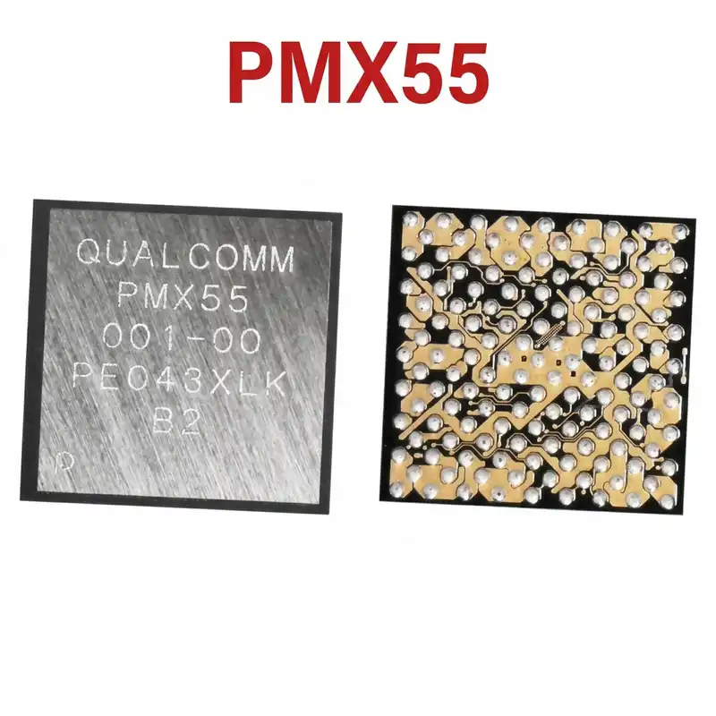
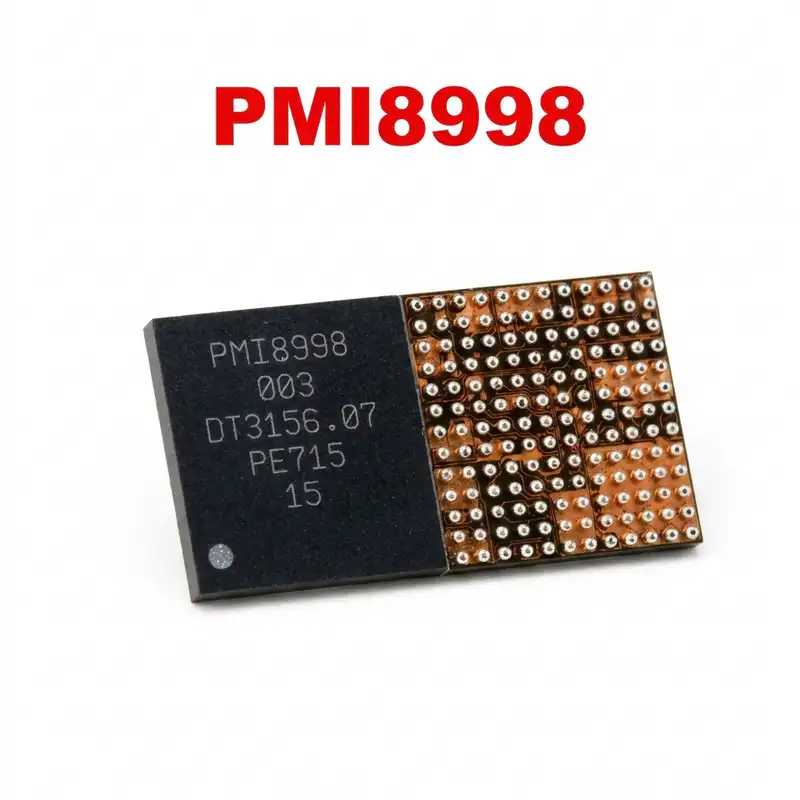
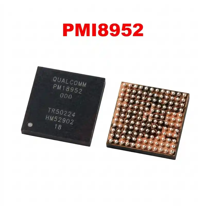
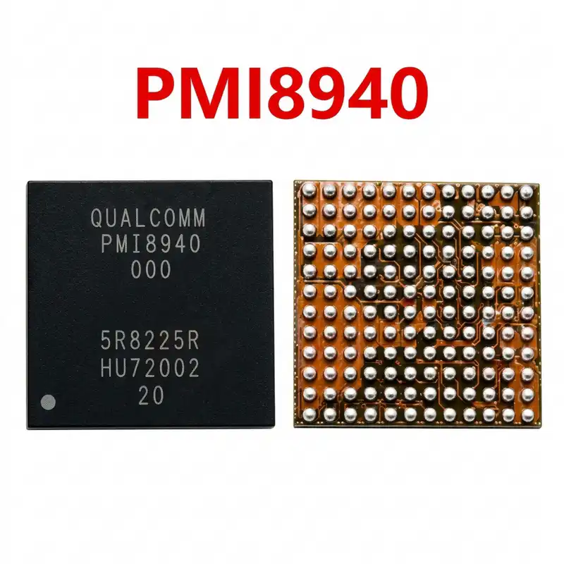
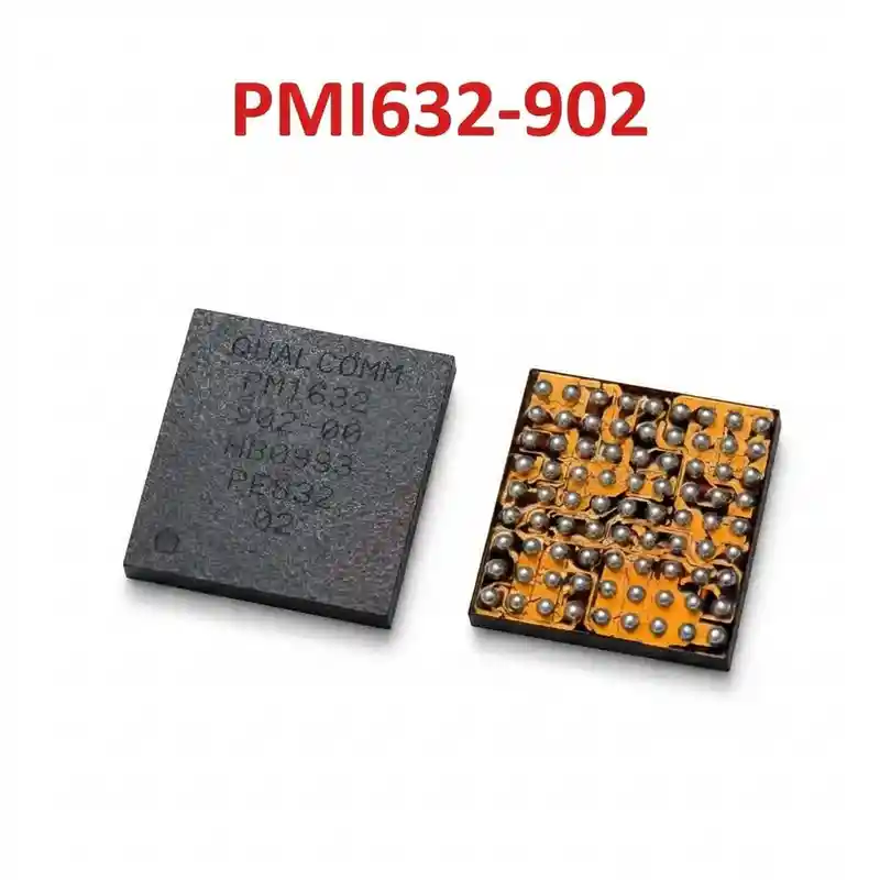
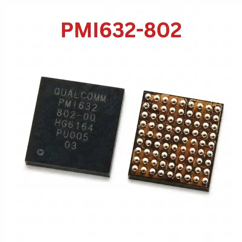
PM8350 IC
As low as
Rs 280.00
Worldwide shipping · Cash on Delivery
Product Details
====================================================================================================
QUALCOMM PM8350-004 / PM8350 004 SNAPDRAGON 888 MASTER PMIC REPAIR GUIDE
====================================================================================================
1. PRODUCT IDENTIFICATION & SILICON SPECIFICATIONS:
----------------------------------------------------------------------------------------------------
- Silicon Laser Marking: PM8350 (Production Code: PM8350-004 / PM8350 004)
- Silicon Manufacturer: Qualcomm Technologies, Inc.
- Semiconductor Node: Samsung 5nm EUV Advanced FinFET Architecture
- System Classification: Primary Master Core Power Management Integrated Circuit (Core PMIC)
- Associated SoC Platforms: Qualcomm Snapdragon 888 5G (SM8350), Snapdragon 888+ 5G (SM8350-AC)
- Multi-PMIC Triad Architecture: PM8350-004 (Master) + PM8350C (GPU/Aux) + PM8350BH/BHS (Charger/VPH)
- Package Form Factor: 144-Pin Fine-Pitch Wafer-Level Chip-Scale BGA (WLCSP)
- Regulated Output Domains:
* Multi-Phase Synchronous Step-Down Buck Regulators:
- VDD_CPU_PRIME (Cortex-X1 Super Core up to 3.0GHz): 0.65V – 1.15V Dynamic Voltage Scaling (DVS).
- VDD_CPU_GOLD (Cortex-A78 Performance Cluster): 0.65V – 1.05V DVS.
- VDD_CPU_SILVER (Cortex-A55 Efficiency Cluster): 0.55V – 0.90V DVS.
- VDD_MEM (LPDDR5 High-Frequency Memory Rail): Clean 1.125V / 0.6V VDDQ.
- VDD_MODEM (Snapdragon X60 5G Baseband Core): 0.70V – 0.85V.
* 30+ Precision Ultra-Low Noise Linear LDO Regulators:
- Dedicated clean supplies for UFS 3.1 storage (2.95V VCC, 1.8V VCCQ, 1.2V VCCQ2).
- Multi-channel Camera Sensor rails (AVDD 2.8V, DVDD 1.1V, OIS 3.3V).
- Display interface, touch controller, and high-speed PCIe peripheral power lines.
* Clocks & System Reset Monitoring:
- Integrated 38.4MHz base clock crystal (XO) oscillator driver.
- Power Key debounce circuit (KYPD_PWR_N).
- Cold boot reset tree generator (PON_RESET_N) and continuous PS_HOLD (1.8V) verification.
2. COMPATIBLE 5G FLAGSHIP SMARTPHONES:
----------------------------------------------------------------------------------------------------
- Samsung (Qualcomm Snapdragon 888 Models):
* Galaxy S21 5G (SM-G991U), Galaxy S21+ 5G (SM-G996U), Galaxy S21 Ultra 5G (SM-G998U)
* Galaxy S21 FE 5G (SM-G990U / SM-G990U1)
* Galaxy Z Fold 3 5G (SM-F926U), Galaxy Z Flip 3 5G (SM-F711U)
- Xiaomi:
* Xiaomi Mi 11, Mi 11 Pro, Mi 11 Ultra, Mi 11i
* Mi MIX 4, Mi MIX FOLD
* Redmi K40 Pro / Redmi K40 Pro+
- OnePlus & Oppo:
* OnePlus 9, OnePlus 9 Pro, OnePlus 9RT
* Oppo Find X3 Pro, Oppo Find X5 (Snapdragon 888 edition)
- Gaming & Performance Flagships:
* ASUS ROG Phone 5 / 5s, Black Shark 4 Pro, Red Magic 6 / 6 Pro, Realme GT 5G, Vivo X60 Pro+ / iQOO 7 / iQOO 8
3. TYPICAL BOARD-LEVEL FAULT SYMPTOMS:
----------------------------------------------------------------------------------------------------
- Completely Dead Logic Board (Stuck Current 0.08A – 0.15A on DC Power Supply):
* Upon pressing the power button, the DC bench supply jumps to ~80mA–150mA and hangs indefinitely.
* Cause: Missing Cortex-X1 or A78 core buck voltages, defective 38.4MHz sleep clock oscillation,
or failed SPMI digital handshaking with companion PM8350C / PM8350BH.
- Automatic Emergency Download Mode (Qualcomm HS-USB QDLoader 9008):
* Handset stays on a black screen and connects directly to PC in 9008 mode. Caused by missing or
unstable UFS 3.1 storage power rails (2.95V / 1.8V / 1.2V) generated by PM8350-004.
- Thermal Cycling Failure / Rebooting Under Load (Snapdragon 888 Thermal Stress):
* The 5nm Snapdragon 888 generates substantial heat. Thermal expansion and contraction over time
frequently cause micro-fractures under the BGA solder balls of PM8350, triggering random reboots
or sudden shutdowns during 3D gaming or 4K/8K camera recording.
- Primary VPH_PWR Line Short Circuit:
* High-side buck MOSFET breakdown inside PM8350-004 shorts the motherboard's main 4.0V VPH_PWR rail
directly to ground (0.000V in diode mode), causing the bench power supply to trip overcurrent protection.
4. STEP-BY-STEP MULTIMETER TESTING & DIAGNOSTICS:
----------------------------------------------------------------------------------------------------
A. Cold Testing (Diode Mode Check - Board Powered Off):
1. Place digital multimeter in Diode Mode. Connect RED probe to motherboard GND shield:
- Main VPH_PWR Input Bypass Capacitors: Normal ~360mV – 480mV.
- Cortex-X1 Prime Core Inductor: Normal ~18mV – 50mV (ultra-low impedance; must NOT read 0.000V).
- Cortex-A78 Gold Core Inductors: Normal ~25mV – 65mV.
- LPDDR5 Memory Buck Inductor: Normal ~220mV – 320mV.
- UFS Storage LDO Output Capacitors: Normal ~380mV – 520mV.
- SPMI Bus Clock & Data Lines: Normal ~450mV – 540mV (must be closely matched within 15mV).
2. Short-Circuit Isolation:
- If VPH_PWR reads 0.000V, inject 3.8V DC (limited to 2.5A) with thermal imaging or rosin vapor.
If PM8350-004 glows bright white, lift the IC to clear the short.
B. Live Operating Voltage Check (Hot Testing):
1. Connect DC power supply at 4.0V to battery terminals.
2. Verify steady 4.0V VPH_PWR on bypass capacitors surrounding PM8350-004.
3. Check Power Key contact: Must measure steady 1.8V DC.
4. Press Power Button and measure output inductors during startup:
- CPU Core inductors must output 0.75V – 0.95V DC.
- LPDDR5 rail must generate steady 1.125V DC.
- Verify PS_HOLD line: Must rise from 0V to 1.8V and lock high. If PS_HOLD drops back to 0V
after 1–2 seconds, inspect the UFS 3.1 storage and CPU/RAM dual-stack solder joints.
5. SOLDERING, REBALLING & REWORK SPECIFICATIONS:
----------------------------------------------------------------------------------------------------
- Extreme Thermal Sensitivity (5nm Multi-Layer PCB):
* Modern 5nm logic boards use dense, ultra-thin multi-layer copper planes. Excessive heat will cause
inter-layer blistering or bridge the solder balls under the adjacent Snapdragon 888 CPU and RAM.
* Always mask the neighboring CPU, RAM, UFS, and secondary PMICs with multi-layer Kapton tape and
thick copper heatsink coins.
- IC Removal:
* Apply high-grade, non-corrosive RMA tacky BGA flux around PM8350-004.
* Hot air station settings: 315°C – 325°C with 35% – 45% airflow.
* Move nozzle in uniform concentric circles. Once all solder balls liquefy, lift vertically with fine tweezers.
- Pad Preparation & Cleaning:
* Solder-wick the PCB pads flat using copper braid and an iron tip set to 290°C – 300°C.
* Clean thoroughly with 99% Isopropyl Alcohol (IPA) and verify under microscope for any lifted pads.
- Reballing Procedure:
* Use a dedicated 0.12mm middle-layer stencil compatible with Qualcomm PM8350 / SM8350.
* Apply 183°C (Sn63/Pb37) leaded solder paste evenly. Heat gently at 290°C until all 144 balls form uniform spheres.
- Alignment & Installation:
* Apply a microscope-thin film of flux to motherboard pads.
* Align Pin 1 dot precisely with the PCB orientation marking.
* Reflow at 305°C – 315°C until the IC naturally self-centers on solder surface tension.
* Allow motherboard to cool naturally for at least 5 minutes before applying DC power.
====================================================================================================
You may also like