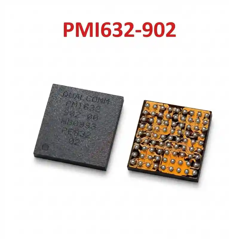
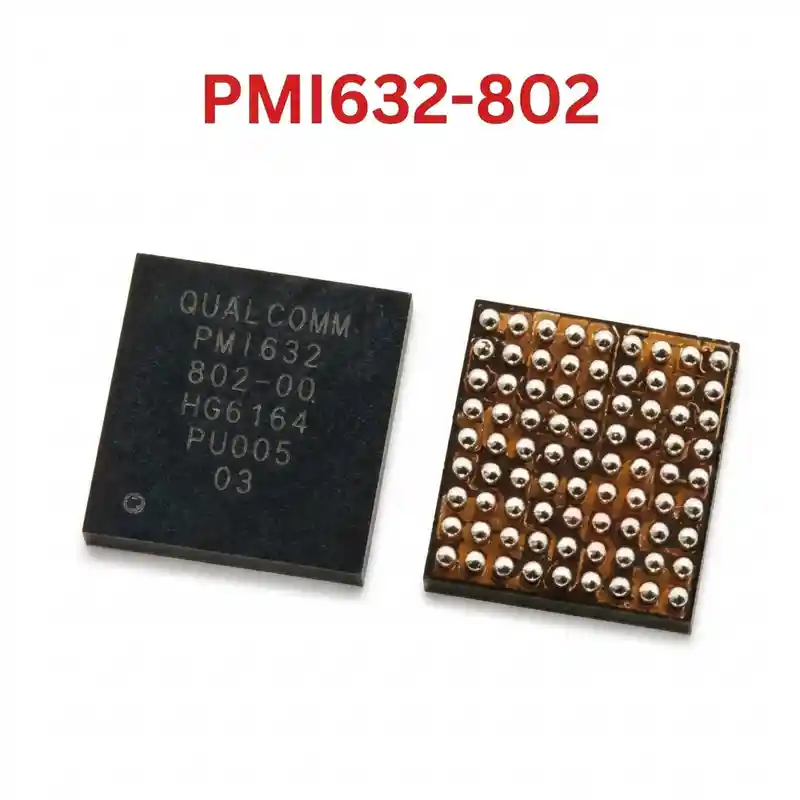
PM8250 IC
As low as
Rs 280.00
Worldwide shipping · Cash on Delivery
Product Details
====================================================================================================
QUALCOMM PM8250 / PM8250-003 SNAPDRAGON 865/870 MASTER PMIC REPAIR GUIDE
====================================================================================================
1. PRODUCT IDENTIFICATION & SILICON SPECIFICATIONS:
----------------------------------------------------------------------------------------------------
- Silicon Laser Marking: PM8250 (Standard Commercial Revision: PM8250-003 / PM8250 003)
- Silicon Manufacturer: Qualcomm Technologies, Inc.
- Package Form Factor: Wafer-Level Chip-Scale BGA (WLCSP / Multi-Ball Array BGA)
- System Hierarchy: Primary Master System Core PMIC (Power Supervisor)
- Primary Associated Platforms: Snapdragon 865 (SM8250), Snapdragon 865+ (SM8250-AB),
Snapdragon 870 (SM8250-AC)
- Companion PMICs in Platform: PM8150B (Charger/VPH PMIC), PM8009 (Camera/Aux PMIC), PM8150L (GPU PMIC)
- Regulated Output Domains:
* Multi-Phase Synchronous Step-Down Buck Converters:
- VDD_APC0 (Kryo 585 Silver Efficiency Cores): ~0.65V – 0.95V Dynamic Voltage Scaling (DVS).
- VDD_APC1 (Kryo 585 Gold / Prime Cortex-A77 Cores up to 3.2GHz): ~0.75V – 1.15V DVS.
- VDD_MEM (LPDDR5 / LPDDR4X Memory Rails): Clean 1.125V / 0.6V VDDQ.
- VDD_MODEM / CORE: Dynamic baseband logic power (~0.75V – 0.90V).
* 25+ Precision Ultra-Low Noise Linear LDO Regulators:
- Dedicated clean supplies for UFS 3.1 storage (2.95V VCC, 1.8V VCCQ, 1.2V VCCQ2).
- Camera image sensor supplies (AVDD 2.8V, DVDD 1.1V).
- Display interface, touch controller, and analog sensory subsystem supplies.
* System Clocks & Master Reset Supervision:
- Integrated 38.4MHz base clock crystal (XO) oscillator driver.
- Hardware debounce logic for Power Key (KYPD_PWR_N).
- Primary power-on reset generator (PON_RESET_N) and continuous PS_HOLD (1.8V) verification.
2. COMPATIBLE SMARTPHONE LOGIC BOARDS:
----------------------------------------------------------------------------------------------------
- Samsung (Qualcomm Snapdragon 865 Editions):
* Galaxy S20, S20+, S20 Ultra: SM-G981U, SM-G986U, SM-G988U
* Galaxy S20 FE 5G: SM-G781B, SM-G781U
* Galaxy Note 20, Note 20 Ultra: SM-N981U, SM-N986U
* Galaxy Z Flip 5G (SM-F707U), Galaxy Z Fold 2 (SM-F916U)
- Xiaomi / Poco:
* Poco F3 / Redmi K40 (Snapdragon 870)
* Xiaomi Mi 10, Mi 10 Pro, Mi 10 Ultra
* Xiaomi Mi 10T, Mi 10T Pro
* Redmi K30 Pro / Poco F2 Pro
* Xiaomi Pad 5 Pro
- OnePlus:
* OnePlus 8, OnePlus 8 Pro, OnePlus 8T, OnePlus 9R
- Gaming & Flagship Devices:
* ASUS ROG Phone 3, Black Shark 3 / 3 Pro, Black Shark 4, Realme GT Neo 2, Vivo iQOO 3 / Neo 5, Motorola Edge Plus
3. TYPICAL BOARD-LEVEL FAULT SYMPTOMS:
----------------------------------------------------------------------------------------------------
- Completely Dead Device (0.00A or Stuck Low Current Draw ~0.05A – 0.08A):
* Pressing the power button yields zero reaction or current draws 50mA–80mA and hangs permanently.
* Cause: Missing CPU APC core buck rails, defective 38.4MHz sleep clock oscillation, or missing
cold-boot reset preventing the Snapdragon 865/870 processor from taking over the power tree.
- Direct Emergency Download Mode (Qualcomm HS-USB QDLoader 9008):
* Phone displays a permanent black screen; when connected to a PC via USB, it enumerates directly as
"Qualcomm HS-USB QDLoader 9008". Caused by missing or unstable UFS 3.1 storage power rails from PM8250.
- Immediate Crash / Reboot Under 3D Gaming or Heavy Processing:
* Phone boots to home screen and handles basic tasks normally, but launching 3D games or running
benchmarks triggers an immediate shutdown due to voltage sag on the Kryo 585 Gold/Prime buck coils.
- Primary VPH_PWR Short Circuit:
* Internal breakdown of PM8250's high-side power MOSFET pulls the motherboard's main 4.0V VPH_PWR bus
directly to ground (0.000V in diode mode), causing the bench power supply to trip overcurrent protection.
4. STEP-BY-STEP MULTIMETER TESTING & DIAGNOSTICS:
----------------------------------------------------------------------------------------------------
A. Cold Testing (Diode Mode Check - Board Powered Off):
1. Place Multimeter in Diode Mode. Connect RED probe to motherboard GND shield:
- Main VPH_PWR Input Capacitors next to PM8250: Normal ~360mV – 480mV.
- CPU Core Buck Inductors (APC0 / APC1): Normal ~20mV – 65mV (ultra-low resistance core; must NOT read 0.000V).
- LPDDR5 Memory Buck Inductor (VDD_MEM): Normal ~240mV – 340mV.
- UFS Storage LDO Output Capacitors: Normal ~380mV – 520mV.
- Power Key Pin: Normal ~600mV – 750mV.
2. Short-Circuit Isolation:
- If VPH_PWR reads 0.000V, inject 3.8V DC (limited to 2.5A) with thermal imaging or rosin vapor.
If PM8250 glows white hot immediately, remove the IC to clear the short.
B. Live Operating Voltage Check (Hot Testing):
1. Connect DC power supply at 4.0V to battery terminals.
2. Verify steady 4.0V VPH_PWR on bypass capacitors surrounding PM8250.
3. Check Power Key pin: Must measure steady 1.8V DC.
4. Press Power Key and measure output inductors during boot sequence:
- CPU Core inductors must output 0.75V – 0.90V DC.
- Memory rail (VDD_MEM) must generate steady 1.125V DC.
- Verify PS_HOLD line: Must rise from 0V to 1.8V and stay locked high. If PS_HOLD drops back
to 0V after 1–2 seconds, inspect UFS 3.1 storage and CPU/RAM solder integrity.
5. SOLDERING, REBALLING & REWORK SPECIFICATIONS:
----------------------------------------------------------------------------------------------------
- Thermal Shielding Precautions:
* On Snapdragon 865/870 boards, PM8250 is positioned near the CPU/RAM layered package and UFS storage.
* Always mask the neighboring CPU, RAM, and storage with multi-layer Kapton tape and thick copper/aluminum
heatsink shields to prevent collateral solder ball bridging under the processor.
- IC Removal:
* Apply premium non-corrosive RMA tacky BGA flux around PM8250.
* Hot air station settings: 315°C – 325°C with 40% – 50% airflow.
* Move nozzle in uniform circular paths. Once all solder balls liquefy, lift vertically with fine micro-tweezers.
- Pad Preparation & Cleaning:
* Solder-wick the PCB pads flat using copper desoldering braid and an iron tip set to 290°C – 300°C.
* Clean thoroughly with 99% Isopropyl Alcohol (IPA) and inspect pads under microscope.
- Reballing Procedure:
* Use a dedicated 0.12mm stencil compatible with Qualcomm PM8250 / SM8250.
* Apply 183°C (Sn63/Pb37) leaded solder paste evenly. Heat gently at 290°C until uniform spheres form.
- Re-installation:
* Apply an ultra-thin film of flux to motherboard pads.
* Align Pin 1 dot with the PCB corner orientation marking. Reflow at 305°C – 315°C until the IC naturally self-centers.
* Allow motherboard to cool naturally for at least 5 minutes before applying DC power.
====================================================================================================
You may also like