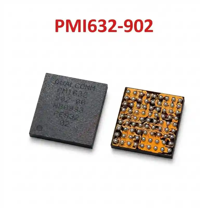
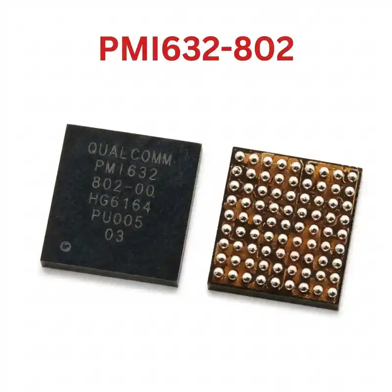
PM8150A IC
As low as
Rs 200.00
Worldwide shipping · Cash on Delivery
Product Details
====================================================================================================
QUALCOMM PM8150A / PM8150A-102 SECONDARY AUXILIARY PMIC REPAIR GUIDE
====================================================================================================
1. PRODUCT IDENTIFICATION & SILICON SPECIFICATIONS:
----------------------------------------------------------------------------------------------------
- Silicon Laser Marking: PM8150A (Production Revision Code: PM8150A-102)
- Silicon Manufacturer: Qualcomm Technologies, Inc.
- Functional Role: Secondary / Auxiliary Power Management IC (Sub-PMIC)
- Package Form Factor: Fine-Pitch Wafer-Level Chip-Scale BGA (WLCSP)
- System Control Protocol: High-Speed SPMI (System Power Management Interface) slave node
- Multi-PMIC Architecture: Paired with PM8150 (Master PMIC) and PM8150B (Charger/Interface PMIC)
- Associated SoC Platforms: Snapdragon 855 (SM8150), Snapdragon 855+ (SM8150-AC),
Snapdragon 860 (SM8150-Pro), Snapdragon 865 (SM8250)
- Regulated Output Domains:
* Synchronous Step-Down Buck Converters:
- Dedicated clean supplies feeding secondary system domains, baseband core, and PCIe controllers.
* Ultra-Low Noise Linear LDO Regulators:
- Clean supply rails dedicated to RF Transceiver ICs (SDR8150).
- Multi-rail Camera Sensor power (AVDD 2.8V, DVDD 1.1V/1.2V).
- Wi-Fi 6 / Bluetooth 5.1/5.2 subsystem power (WCN3998 / WCN6850).
- Sensory hub, display interface, and touch controller auxiliary power lines.
2. COMPATIBLE SMARTPHONE LOGIC BOARDS:
----------------------------------------------------------------------------------------------------
- Samsung (Qualcomm Snapdragon Editions):
* Galaxy S10 / S10+ / S10e: SM-G973U, SM-G975U, SM-G970U, SM-G977U (S10 5G)
* Galaxy Note 10 / Note 10+: SM-N970U, SM-N975U, SM-N976U (Note 10 5G)
* Galaxy S20 / S20+ / S20 Ultra: SM-G981U, SM-G986U, SM-G988U
* Galaxy S20 FE 5G: SM-G781B, SM-G781U
- Xiaomi / Poco:
* Poco X3 Pro (Bhima / Vayu - Snapdragon 860)
* Xiaomi Mi 9, Mi 9 Pro 5G, Xiaomi Mi 10, Mi 10 Pro
* Redmi K20 Pro / Mi 9T Pro
- OnePlus:
* OnePlus 7, OnePlus 7 Pro, OnePlus 7T, OnePlus 7T Pro
* OnePlus 8, OnePlus 8 Pro, OnePlus 8T
- Motorola / Oppo:
* Motorola Edge Plus, Moto Z4
* Oppo Reno 10X Zoom
3. TYPICAL BOARD-LEVEL FAULT SYMPTOMS:
----------------------------------------------------------------------------------------------------
- Completely Dead Logic Board (Stuck Current 0.07A – 0.12A on DC Bench Supply):
* Upon pressing the power button, current draws a steady 70mA–120mA and hangs permanently.
* The Master PMIC (PM8150) powers up, but SPMI initialization stalls because PM8150A fails to report
"Power Good", prompting the CPU to halt the boot progression.
- Cellular Baseband Failure ("No Service" / "Searching" / Unknown Baseband):
* Phone turns on normally, but cannot connect to mobile network; IMEI or Baseband version missing in
settings due to absent RF transceiver (SDR8150) voltage rails.
- Wi-Fi / Bluetooth Toggle Greyed Out:
* Wi-Fi button cannot be turned on in settings due to collapsed 1.8V / 3.3V LDO rails feeding the WCN chip.
- Camera Subsystem Failure / Immediate App Crash:
* Launching Camera app yields a black screen or "Camera Failed" error due to missing AVDD 2.8V line.
- Primary VPH_PWR Line Short Circuit:
* Internal high-side buck MOSFET failure shorts the motherboard's main 4.0V VPH_PWR rail directly to ground
(0.000V in diode mode), causing the bench power supply to trip overcurrent protection instantly.
4. STEP-BY-STEP MULTIMETER TESTING & DIAGNOSTICS:
----------------------------------------------------------------------------------------------------
A. Cold Testing (Diode Mode Check - Board Powered Off):
1. Select Diode Mode on digital multimeter. Connect RED probe to motherboard GND shield:
- Main VPH_PWR Input Capacitors next to PM8150A: Normal ~360mV – 480mV.
- Output Buck Inductors: Normal ~180mV – 320mV (must NOT read 0.000V).
- RF Transceiver Power LDO Caps (SDR8150 supply lines): Normal ~420mV – 580mV.
- SPMI Clock & Data Lines: Normal ~460mV – 540mV (must be closely matched within 15mV).
- Wi-Fi 1.8V / 3.3V Power Caps: Normal ~380mV – 520mV.
2. Short-Circuit Isolation:
- If VPH_PWR reads 0.000V, inject 3.8V DC (limited to 2.5A) with rosin smoke or a thermal camera.
If PM8150A glows white immediately, lift the IC to clear the short.
B. Live Operating Voltage Check (Hot Testing):
1. Connect DC power supply at 4.0V to battery terminals.
2. Verify steady 4.0V VPH_PWR input on the bypass capacitors surrounding PM8150A.
3. Press Power Button and test output rails during startup:
- Buck inductors around PM8150A must pulse to their operating voltages (~0.85V – 1.2V).
- SPMI clock and data lines must hold stable 1.8V DC.
4. Launch Camera and Wi-Fi and verify:
- Camera connector power pins should register active 2.8V AVDD.
- Wi-Fi supply lines should show active 1.8V/3.3V. If absent, replace PM8150A.
5. SOLDERING, REBALLING & REWORK SPECIFICATIONS:
----------------------------------------------------------------------------------------------------
- Thermal Shielding:
* Protect adjacent Snapdragon 855 / 860 / 865 CPU, UFS storage, and SDR8150 transceiver with multi-layer
Kapton tape and thick aluminum heatsink foil to prevent collateral solder ball bridging.
- IC Removal:
* Apply premium non-corrosive RMA tacky BGA flux around PM8150A.
* Hot air station settings: 315°C – 325°C with 40% – 50% airflow.
* Heat in even circular motions. Once all solder balls liquefy, lift vertically with fine micro-tweezers.
- Pad Preparation & Cleaning:
* Solder-wick the PCB pads flat using copper desoldering braid and an iron tip set to 290°C – 300°C.
* Clean thoroughly with 99% Isopropyl Alcohol (IPA) and verify under microscope for any lifted pads.
- Reballing Procedure:
* Use a dedicated 0.12mm stencil compatible with Qualcomm PM8150 / PM8150A / SM8150.
* Apply 183°C (Sn63/Pb37) leaded solder paste evenly. Heat gently at 290°C until uniform spheres form.
- Re-installation:
* Apply a microscope-thin film of flux to motherboard pads.
* Align Pin 1 dot with the PCB silkscreen orientation marking.
* Reflow at 305°C – 315°C until the IC naturally self-centers on solder surface tension.
* Allow motherboard to cool naturally for at least 5 minutes before applying DC power.
====================================================================================================
You may also like