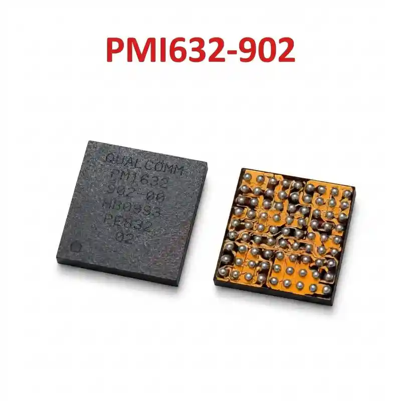
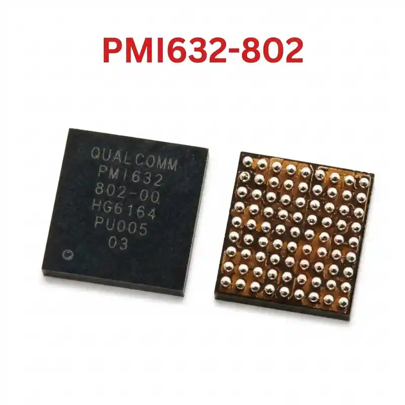
PM8029 IC
As low as
Rs 280.00
Worldwide shipping · Cash on Delivery
Product Details
====================================================================================================
QUALCOMM PM8029 (PM-8029-0-140WLNSP) MASTER PMIC REPAIR & REWORK GUIDE
====================================================================================================
1. PRODUCT IDENTIFICATION & SILICON SPECIFICATIONS:
----------------------------------------------------------------------------------------------------
- Silicon Laser Marking: PM8029
- Full Manufacturer Part Number: PM-8029-0-140WLNSP-TR-01-0
- Silicon Manufacturer: Qualcomm Technologies, Inc.
- Package Form Factor: 140-Ball Wafer-Level Nano-Scale Package (140 WLNSP / BGA)
- System Classification: Primary All-in-One Master Power Management IC (Power Supervisor)
- Primary Target SoC Platforms: Qualcomm Snapdragon S4 Play / Snapdragon 200
(MSM8225, MSM8625, MSM8225Q, MSM7227A, MSM7627A)
- Core Regulated Output Domains:
* Synchronous Step-Down Buck Converters:
- VDD_MSMC1 / MSMC2: CPU Core Supply (~1.05V – 1.25V Dynamic Voltage Scaling for Cortex-A5).
- VDD_MEM: LPDDR / LPDDR2 Memory Supply (1.2V / 1.8V).
* Linear Low-Dropout (LDO) Regulators:
- VREG_MSMA (Analog Core): 1.8V.
- VREG_NAND / EMMC: 2.85V VDD supply and 1.8V VIO peripheral I/O supply.
- Display LCD Bias & Touchscreen LDOs: Clean 2.8V – 3.0V rails.
- Camera Sensor Supplies: 2.8V AVDD, 1.2V DVDD, and 1.8V DOVDD.
* Power Sequencing & System Clock:
- Manages RTC oscillator circuit (32.768kHz sleep crystal).
- Power Key Detection (KYPD_PWR_N) with hardware debounce circuit.
- Reset generation (PS_HOLD verification from MSM).
* Integrated Battery Charging Circuit:
- Linear/switch battery charger handling USB VBUS (5.0V) down to VBAT (4.2V max).
2. COMPATIBLE SMARTPHONE LOGIC BOARDS:
----------------------------------------------------------------------------------------------------
- Samsung:
* Galaxy Grand Quattro / Galaxy Win: GT-I8552, GT-I8550
* Galaxy Core: GT-I8262, GT-I8262D, GT-I8260
* Galaxy S Duos / Trend: GT-S7562, GT-S7560, GT-S7562i
* Galaxy Young / Young Duos: GT-S6310, GT-S6312
* Galaxy Ace Plus: GT-S7500
* Galaxy Mini 2: GT-S6500
- Huawei:
* Ascend G510 (U8951), Ascend Y300 (U8833), Ascend G330D (U8825D), Ascend G730-C00, Honor C8812
- HTC:
* Desire V (T328w), Desire VC (T328d), Desire 600 Dual, Desire 608t
- Nokia / Microsoft:
* Nokia X (RM-980), Nokia Lumia 610
- Sony:
* Xperia J (ST26i / ST26a), Xperia Tipo (ST21i), Xperia Miro (ST23i)
- Motorola:
* Motoluxe (XT615)
3. TYPICAL BOARD-LEVEL FAULT SYMPTOMS:
----------------------------------------------------------------------------------------------------
- Handset Completely Dead (0.00A or Stuck Low Current Draw ~0.03A – 0.06A):
* Pressing power button yields no vibration or display; bench power supply draws a steady 30mA – 60mA
and hangs indefinitely.
* Cause: Missing CPU core buck voltage (VDD_MSMC) or defective 32.768kHz sleep crystal preventing
the MSM processor from completing hardware reset.
- Constant Bootloop / Restarting on Brand Logo:
* Device powers up, displays Samsung / Huawei logo, and immediately reboots or shuts down.
* Common cause: Solder micro-fractures under PM8029's CPU buck ball array or a defective buck filter inductor.
- Fake Charging / No USB Current Ingestion:
* Lightning/charging bolt icon displays on screen, but USB current meter draws 0.00A; battery drains
instead of charging due to burned internal charging pass FETs in PM8029.
- Full Motherboard Short Circuit (VBAT to Ground):
* Internal breakdown of PM8029's battery input pin pulls the battery positive terminal (VBAT) straight
to ground (0.000V in diode mode), causing bench supply to trip instantly.
4. STEP-BY-STEP MULTIMETER TESTING & DIAGNOSTICS:
----------------------------------------------------------------------------------------------------
A. Cold Testing (Diode Mode Check - Board Powered Off):
1. Select Diode Mode on digital multimeter. Connect RED probe to motherboard GND shield:
- Battery Positive Connector Terminal (VBAT): Normal ~450mV – 550mV.
- VREG_MSMC CPU Core Inductor: Normal ~120mV – 220mV (must NOT read 0.000V).
- VREG_MEM Inductor: Normal ~320mV – 450mV.
- Power Key Pin (KYPD_PWR_N): Normal ~600mV – 750mV.
- USB VBUS 5V Input Pin: Normal ~500mV – 650mV.
2. Short-Circuit Isolation:
- If VBAT reads 0.000V, inject 3.8V DC (limited to 2.0A) onto VBAT using rosin vapor or a thermal camera.
If PM8029 heats up immediately, remove the IC to clear the short.
B. Live Operating Voltage Check (Hot Testing):
1. Connect DC power supply at 3.9V to battery terminals.
2. Measure Power Key contact: Must read steady ~1.8V to 3.0V DC.
3. Press Power Key and measure output rails:
- CPU Core inductor (MSMC) must rise to 1.15V – 1.20V DC.
- Memory rail (VREG_MEM) must read 1.2V / 1.8V DC.
- Check 32.768kHz crystal pins with oscilloscope or frequency counter: Must display clean sine wave.
4. If Power Key drops to 0V when pressed but no buck inductors generate voltage, replace PM8029.
5. SOLDERING, REBALLING & REWORK SPECIFICATIONS:
----------------------------------------------------------------------------------------------------
- Thermal Shielding:
* Protect the adjacent MSM8225 / MSM7227A CPU and eMMC storage chips with thermal Kapton tape and
thick aluminum heatsink foil to prevent collateral desoldering.
- IC Removal:
* Apply non-corrosive RMA tacky BGA flux around PM8029.
* Hot air station settings: 310°C – 320°C with 40% – 50% airflow.
* Heat in even circular motions. Once solder liquefies, lift vertically with fine-tip micro-tweezers.
- Pad Dressing & Cleaning:
* Flatten PCB pads using copper desoldering braid and an iron tip at 290°C – 300°C.
* Clean thoroughly with 99% Isopropyl Alcohol (IPA) and verify under microscope for any lifted pads.
- Reballing Procedure:
* Use a dedicated 0.12mm stencil compatible with Qualcomm PM8029 (140 balls).
* Apply 183°C (Sn63/Pb37) leaded solder paste evenly. Heat gently at 290°C until all spheres form uniformly.
- Re-installation:
* Apply an ultra-thin film of flux to motherboard pads.
* Align Pin 1 dot with the PCB corner indicator. Reflow at 305°C – 315°C until the IC naturally self-centers.
* Allow motherboard to cool completely for 5 minutes before applying DC power.
====================================================================================================
You may also like