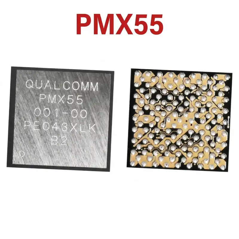
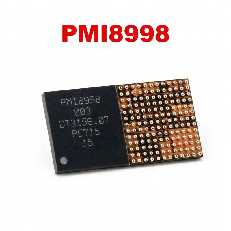
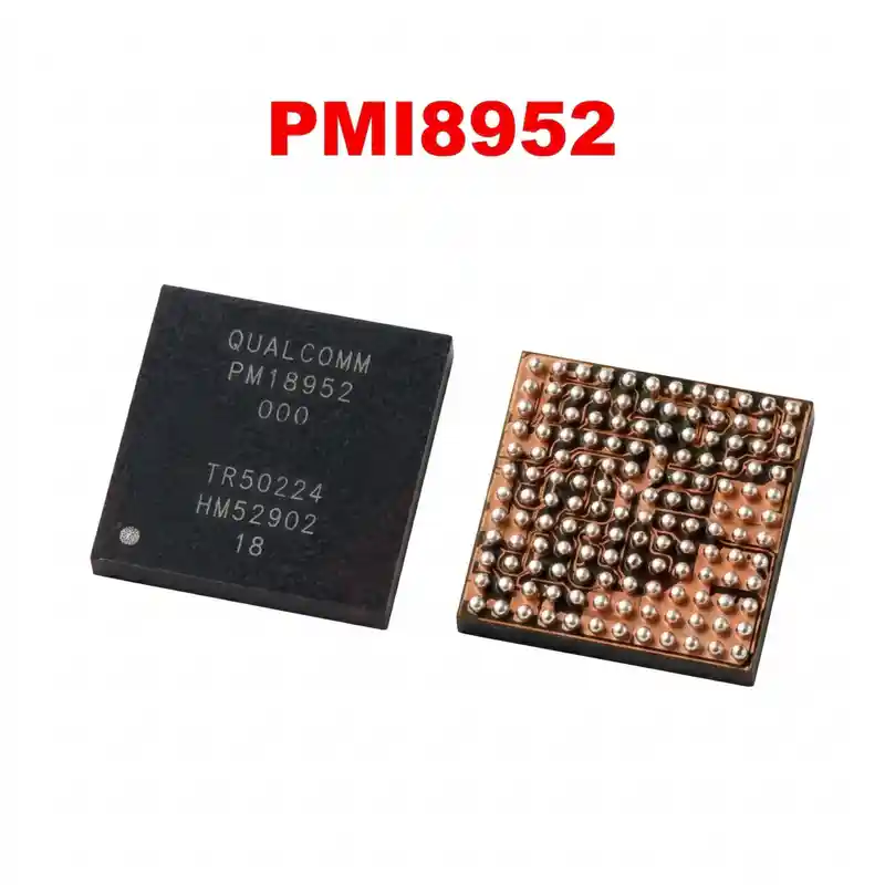
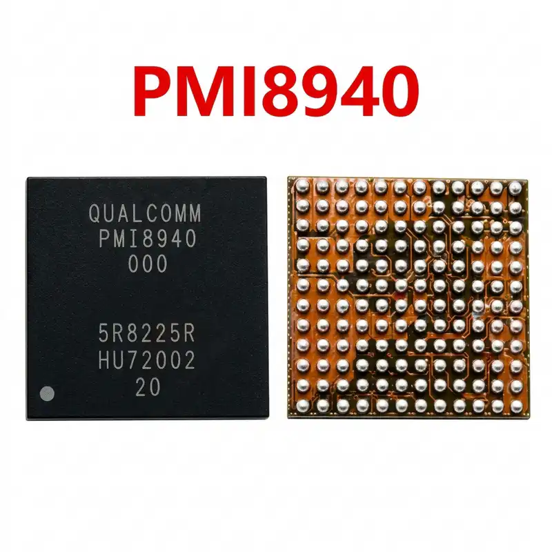
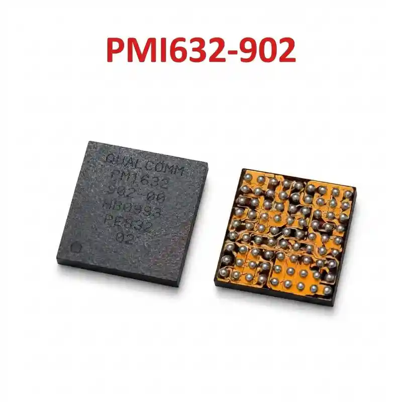
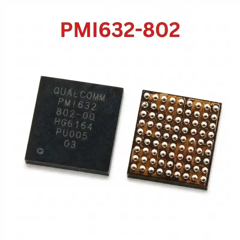
PM7350C IC
As low as
Rs 280.00
Worldwide shipping · Cash on Delivery
Product Details
====================================================================================================
QUALCOMM PM7350C / PM7350C-002 SLAVE / AUXILIARY PMIC REPAIR GUIDE
====================================================================================================
1. PRODUCT IDENTIFICATION & SILICON SPECIFICATIONS:
----------------------------------------------------------------------------------------------------
- Marking Code on Silicon: PM7350C (Standard commercial suffix: 002 / PM7350C-002)
- Silicon Manufacturer: Qualcomm Technologies, Inc.
- Functional Classification: Slave / Auxiliary System PMIC (Sub-PMIC Power Stage)
- Package Form Factor: Wafer-Level Chip-Scale BGA (WLCSP / FOWPSP)
- Control & Interface Bus: High-Speed SPMI (System Power Management Interface) slave node
- Associated SoC Platforms: Snapdragon 780G 5G (SM7350), Snapdragon 778G / 778G+ (SM7325),
Snapdragon 888 (SM8350), and Snapdragon 8-series platforms
- Multi-PMIC Synchronization:
* Master PMIC: PM7325 or PM7350 (Controls Cold Boot, Sleep Clocks, CPU Kryo Cores, Reset)
* Charger PMIC: PM7325B or PM7250B (Controls VBUS Ingestion, Fast Charging, VPH_PWR generation)
* Slave PMIC: PM7350C (Controls GPU dynamic power, Camera ISP, 5G RF Transceiver, UFS Aux)
- Regulated Output Domains:
* Multi-Phase GPU Buck Converter: Powers Adreno GPU core with Dynamic Voltage & Frequency Scaling (DVFS).
* RF & Transceiver Clean LDOs: Ultra-low noise rails for 5G SDR/WTR transceivers and RFFE front-ends.
* Image Signal Processor (ISP) Regulators: Dedicated high-current rails for multi-camera modules.
2. COMPATIBLE SMARTPHONES & LOGIC BOARDS:
----------------------------------------------------------------------------------------------------
- Xiaomi: Mi 11 Lite 5G (Renoir - SM7350), Xiaomi 11T, Xiaomi Civi series
- Samsung: Galaxy A52s 5G (SM-A528B), Galaxy M52 5G (SM-M526B), Galaxy A73 5G, Galaxy S20 FE 5G
- Motorola: Edge 20 Pro (XT2141), Edge 30
- Honor: Honor 50, Honor 60, Honor 70
- Huawei: Nova 9, Nova 10, Nova 11 series (Qualcomm versions)
- Realme: Realme GT Master Edition, Realme GT Neo series
- Vivo: Vivo T1 Pro 5G, iQOO Z5, Vivo X60 series (Snapdragon editions)
3. TYPICAL BOARD-LEVEL FAULT SYMPTOMS:
----------------------------------------------------------------------------------------------------
- Completely Dead Phone (Stuck Current 70mA – 120mA on DC Power Supply):
* When power button is pressed, current jumps to ~70mA–120mA and stays permanently frozen.
* Cause: Master PM7325 powers up, initiates SPMI communication with PM7350C, but PM7350C fails to
acknowledge or release its "Power Good" handshake, causing the AP to abort the boot sequence.
- Immediate Crash / Reboot on Opening Camera App:
* Phone boots and works normally, but opening the Camera app causes the device to immediately shut
down, freeze, or restart due to collapsed ISP / camera sensor LDO rails inside PM7350C.
- Immediate Shutdown / Reboot During 3D Gaming:
* Handset restarts or black-screens the moment a 3D game (PUBG, Genshin Impact) loads. Caused by
voltage collapse on the Adreno GPU buck rail from a degraded PM7350C or cracked solder ball.
- "No Service" / 5G Network Baseband Drop:
* Phone has an IMEI number, but cannot register on cellular networks (searching or no service)
because PM7350C's dedicated RF LDO supplies to the transceiver (SDR735) are missing.
- VPH_PWR Short Circuit / High Heat Generation:
* Physical damage or surge shorting the internal high-side FET pulls the motherboard's main 4.0V
VPH_PWR line to ground, causing instant bench power supply current limit tripping (overcurrent).
4. STEP-BY-STEP MULTIMETER TESTING & DIAGNOSTICS:
----------------------------------------------------------------------------------------------------
A. Cold Testing (Diode Mode Check):
1. Power off board, disconnect battery and USB cables.
2. Place RED probe on GND shield, probe surrounding components with BLACK probe:
- Main VPH_PWR Input Capacitors: Expected 360mV – 480mV.
- GPU Buck Inductor: Expected 35mV – 90mV (naturally low impedance; must NOT read 0.000V).
- Camera ISP Buck/LDO Lines: Expected 320mV – 500mV.
- RF Transceiver Power Lines: Expected 420mV – 600mV.
- SPMI Clock & Data Lines: Expected 450mV – 550mV (must be closely matched).
3. If any coil reads pure 0.000V, inject 1.0V (limited to 2A) on that line to confirm whether PM7350C
or the processor/GPU die is shorted using a thermal camera or rosin smoke.
B. Live Operating Voltages (Hot Testing):
1. Connect DC power supply at 4.0V to battery terminals.
2. Verify VPH_PWR input at PM7350C input bypass capacitors: Must measure solid 4.0V.
3. Press Power Button and measure during the boot cycle:
- Measure GPU buck output: Should briefly rise to ~0.75V – 0.85V during initialization.
- Measure SPMI bus line: Must measure stable 1.8V DC.
4. If Master PM7325 outputs core voltages but PM7350C output coils show 0V, verify SPMI pull-up
resistors (1.8V) before replacing PM7350C.
5. SOLDERING, REBALLING & REWORK SPECIFICATIONS:
----------------------------------------------------------------------------------------------------
- Heat Management & Component Shielding:
* Always mask the neighboring Snapdragon processor, UFS storage, and RF transceiver with multiple
layers of Kapton tape and copper shielding foil to prevent collateral desoldering or bubble damage.
- IC Removal:
* Apply premium no-clean RMA tacky flux around PM7350C.
* Set hot air station to 320°C with 40% – 50% airflow.
* Heat evenly in small circles; lift vertically with micro-tweezers as soon as solder liquefies.
- Pad Preparation:
* Clean PCB pads using copper desoldering braid and a micro-chisel soldering iron at 300°C. Clean
thoroughly with 99% Isopropyl Alcohol (IPA) to ensure a perfectly flat, mirrored surface.
- Reballing Procedure:
* Use a dedicated 0.12mm middle-layer stencil compatible with PM7350C / SM7350.
* Use 183°C (Sn63/Pb37) solder paste. Heat smoothly at 290°C – 300°C until all balls form uniformly.
- Re-installation:
* Apply an ultra-thin layer of flux on the PCB pads.
* Align Pin 1 dot precisely with the PCB orientation marking.
* Reflow at 310°C – 320°C until the IC naturally pulls into alignment on its solder surface tension.
* Allow motherboard to cool naturally for at least 5 minutes before applying DC power.
====================================================================================================
You may also like