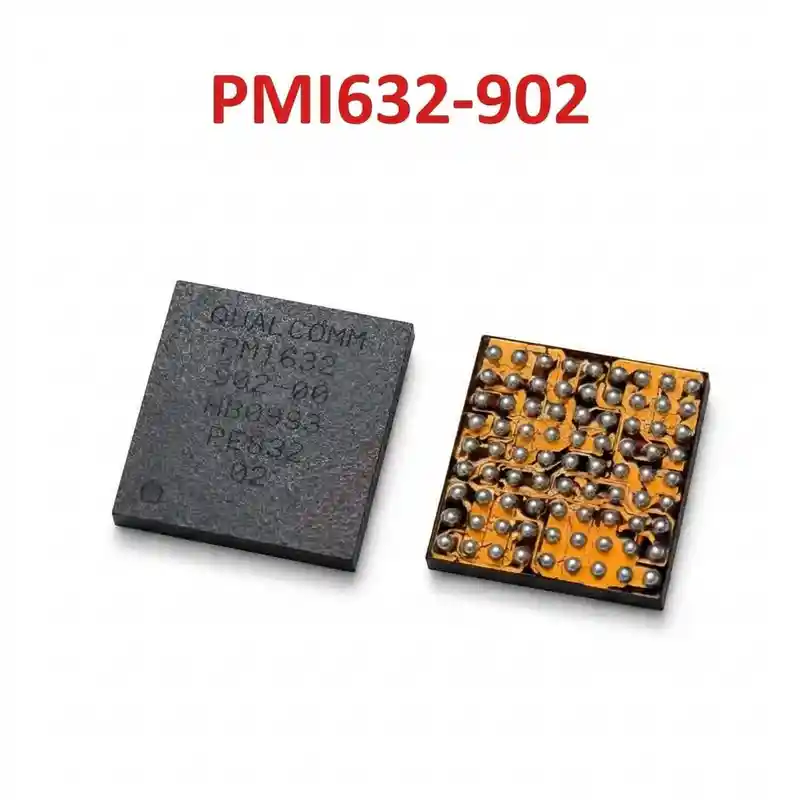
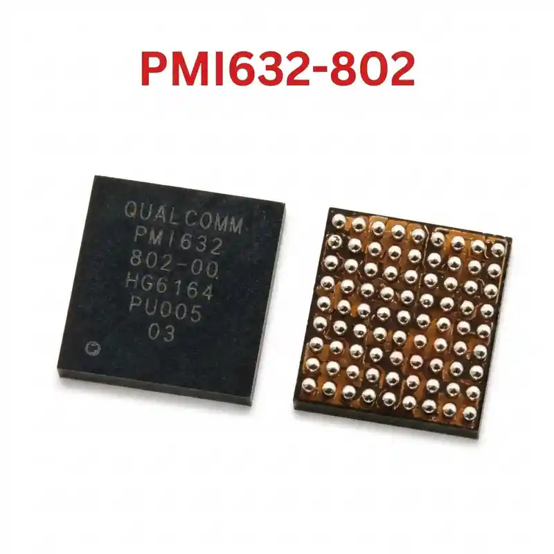
PM660A IC
As low as
Rs 250.00
Worldwide shipping · Cash on Delivery
Product Details
====================================================================================================
QUALCOMM PM660A (001 / 002-01) POWER MANAGEMENT IC COMPREHENSIVE GUIDE
====================================================================================================
1. PRODUCT IDENTIFICATION & SPECIFICATIONS:
----------------------------------------------------------------------------------------------------
- Part Numbers: PM660A, PM660A-001, PM660A-002-01
- Silicon Manufacturer: Qualcomm Technologies, Inc.
- Chipset Family: Qualcomm Snapdragon 636, Snapdragon 660, Snapdragon 670
- Multi-PMIC Architecture: Works in conjunction with PM660 (Primary) and PM660L (Secondary)
- Functional Classification: Auxiliary / System Power Management IC (PMIC)
- Package Type: Fine-Pitch BGA (Ball Grid Array)
- Input Operating Voltage: VPH_PWR (3.4V – 4.35V DC) from system switching node
- Regulated Output Rails:
* Integrated Synchronous Step-Down Buck Regulators:
- Step-down buck converters generating targeted low-voltage, high-current supply rails for
application processor sub-cores, modem digital blocks, and system buses.
* Multi-Channel Low-Dropout (LDO) Regulators:
- Dedicated clean analog rails (1.8V VIO, 2.8V / 2.95V sensor, camera analog, and memory rails).
- Thermal & Solder Parameters:
* Reballing Stencil: Amaoe Qualcomm PM660 / PM660A / PM660L Universal PMIC Stencil (0.12mm)
* Recommended Solder Paste: 183°C Leaded Solder Paste (Sn63/Pb37)
* Hot Air Rework Range: 315°C – 330°C (Airflow: 40% – 50%)
2. MOTHERBOARD ARCHITECTURE & ROLE IN SYSTEM:
----------------------------------------------------------------------------------------------------
- PM660 vs PM660A vs PM660L Subsystem Split:
* PM660: Primary Master PMIC controlling main CPU core rails, RAM power, 38.4MHz oscillator, and reset.
* PM660A: Specialized auxiliary power hub handling specific RF transceiver supplies, auxiliary CPU/
peripheral power domains, and system bus logic in select motherboard layouts.
* PM660L: Secondary PMIC managing battery charging (SMBB/Qnovo), LCD backlight driver, display bias,
and camera flash LEDs.
- Control & Bus Interface:
* SPMI (System Power Management Interface) bidirectional communication bus linked directly to the AP.
* Dedicated enable/reset lines coordinating multi-PMIC power-on state machine sequence.
- Target Compatible Smartphones:
* Xiaomi / Redmi: Redmi Note 5 / Note 5 Pro, Xiaomi Mi Note 3, Mi 6X, Mi A2
* Vivo: Vivo X20, Vivo X20 Plus, Vivo X21, Vivo V11 / V11 Pro
* Oppo: Oppo R11, Oppo R11s, Oppo R11 Plus
* Samsung: Galaxy A8 Star (SM-G885 / G8850 / G885F).
3. COMMON MOTHERBOARD FAULT SYMPTOMS:
----------------------------------------------------------------------------------------------------
- Device Completely Dead (0.00A Current Draw):
* No reaction upon pressing power key; missing initial VREG startup voltages or cracked solder joints.
- Low Current Freeze / Hang (0.03A – 0.07A Current Draw):
* Motherboard powers up slightly upon pressing the power button, draws ~40mA to 70mA on DC power supply,
and locks up permanently without boot progression (indicates missing auxiliary buck or LDO output).
- Qualcomm HS-USB QDLoader 9008 Port Loop:
* Device fails to boot Android OS and automatically enters emergency download (EDL) mode due to
instability on auxiliary storage or digital rail.
- Intermittent Power-Off / Restarts under Load:
* Micro-fractures under BGA solder balls or thermal breakdown inside internal FET switches causing
sudden dropouts when running demanding tasks or 3D graphics.
- VPH_PWR Primary Short Circuit:
* Internal breakdown of buck high-side MOSFETs creating a direct short to ground, causing the DC power
supply to trip immediately upon connecting battery leads.
4. STEP-BY-STEP DIAGNOSIS & TROUBLESHOOTING:
----------------------------------------------------------------------------------------------------
A. Cold Testing (Diode Mode Readings):
1. Disconnect battery and USB charging cable completely.
2. Switch digital multimeter to Diode Mode.
3. Place RED probe on motherboard ground shield (GND).
4. Probe peripheral capacitors and inductors surrounding PM660A:
- Main VPH_PWR filter capacitors: Normal reading 350mV – 480mV.
- Output buck inductors: Normal reading 200mV – 380mV (depending on line impedance).
- LDO bypass output capacitors: Normal reading 300mV – 600mV.
5. If any inductor or capacitor reads 0.000V (beep to ground), isolate the rail with rosin smoke /
thermal imaging at 1.0V – 1.8V to locate the shorted component.
B. Hot Testing (Live Voltage Sequencing):
1. Supply 4.0V DC to battery terminal via stabilized bench power supply.
2. Verify that 4.0V VPH_PWR is present at all input pins of PM660A.
3. Press Power Key to trigger the boot sequence.
4. Monitor regulated outputs across surrounding filter inductors and test points. Ensure voltages
rise cleanly to their nominal target values without oscillations.
5. If input voltage is present but zero output voltages appear upon triggering power key, verify the
SPMI data/clock lines from the processor and check PM660 master enable handshakes.
5. REWORK, REBALLING & REPLACEMENT PROCEDURE:
----------------------------------------------------------------------------------------------------
- Thermal Protection & Shielding:
* Apply polyimide thermal tape and aluminum shielding over nearby CPU/eMMC memory packages and
underfilled sensors to prevent heat damage or solder ball bridging.
- Desoldering & Removal:
* Apply a small amount of non-corrosive BGA flux around the edges of PM660A.
* Use a hot air rework station set at 320°C with 45% airflow.
* Move the nozzle in an even circular pattern around the chip.
* Once the solder balls liquefy, lift the IC vertically using fine curved tweezers.
- Pad Dressing & Cleaning:
* Apply fresh leaded solder paste or flux to motherboard pads.
* Clean pads completely flat using a chisel-tip soldering iron (300°C) and copper solder braid.
* Thoroughly remove flux residue with 99% Isopropyl Alcohol (IPA) and inspect under microscope.
- Reballing & Alignment:
* Place the IC in a 0.12mm dedicated PM660 stencil and scrape 183°C leaded solder paste evenly.
* Heat with hot air station at 280°C – 300°C with low airflow until uniform solder spheres form.
* Apply a micro-layer of flux to PCB pads, align the Pin 1 corner indicator dot accurately with
motherboard silkscreen markings, and heat gently at 310°C until self-alignment occurs.
====================================================================================================
You may also like