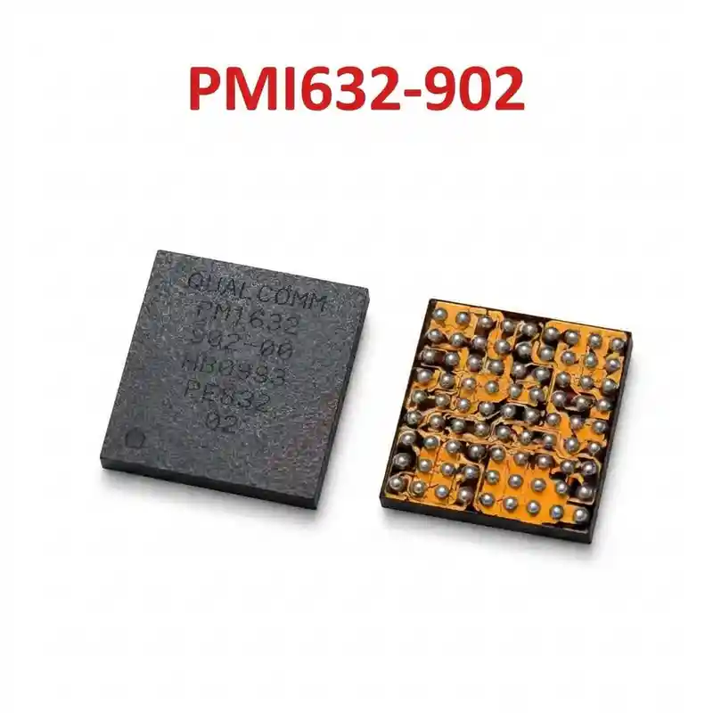
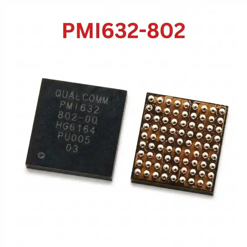
PM6250 IC
As low as
Rs 250.00
Worldwide shipping · Cash on Delivery
Product Details
====================================================================================================
QUALCOMM PM6250-102 SYSTEM POWER MANAGEMENT IC COMPREHENSIVE REPAIR GUIDE
====================================================================================================
1. PRODUCT IDENTIFICATION & HARDWARE SPECIFICATIONS:
----------------------------------------------------------------------------------------------------
- Part Number: PM6250-102 (Laser silkscreen marking on package: PM6250 / 102)
- Related Revisions: PM6250-001 (Qualcomm PM6250 Family)
- Silicon Manufacturer: Qualcomm Technologies, Inc.
- Platform Architectures: Snapdragon 720G (SM7125), Snapdragon 730G (SM7150), Snapdragon 732G
- Multi-PMIC Power Topology: Primary / Subsystem PMIC (Commonly coordinated in multi-PMIC designs)
- Functional Classification: Multi-Channel Step-Down Buck Converter & Precision LDO PMIC
- Package Type: Fine-Pitch Wafer-Level BGA (Ball Grid Array)
- Input Operating Voltage: VPH_PWR (3.4V to 4.35V DC) supplied from primary system switching node
- Regulated Output Rails:
* Synchronous Step-Down Buck Converters:
- High-efficiency dynamic buck regulators supplying low-voltage core power to application processor
processing domains, digital baseband, and modem transceiver subsystems.
* 20+ Precision Low-Dropout (LDO) Regulators:
- Ultra-clean analog supplies for UFS storage (2.95V / 1.8V), System I/O (1.8V VIO),
Camera analog sensors (AVDD 2.8V, DVDD 1.2V), Display interface, and RF PLL rails.
- Thermal & Soldering Guidelines:
* Reballing Stencil: Amaoe Qualcomm SM7125 / SM7150 / PM6250 Dedicated Stencil (0.12mm)
* Recommended Solder Alloy: 183°C Leaded Solder Paste (Sn63/Pb37)
* Hot Air Rework Settings: 315°C – 325°C (Airflow: 40% – 50%)
2. CIRCUIT ARCHITECTURE & MOTHERBOARD ROLE:
----------------------------------------------------------------------------------------------------
- Primary / Subsystem Power Hub:
* In Snapdragon 720G/732G motherboards (e.g., Samsung A52/A72 and Redmi Note series), PM6250 works
to regulate critical system rails, core buck lines, and high-speed peripheral supplies.
* Coordinated directly with the Snapdragon application processor over the bidirectional SPMI serial bus.
* Senses system boot triggers and provides clean, regulated power sequencing to maintain AP stability.
- Target Compatible Smartphones:
* Samsung: Galaxy A52 4G (SM-A525F / A525M), Galaxy A72 4G (SM-A725F / A725M)
* Xiaomi / Redmi: Xiaomi Mi 10, Redmi Note 9 Pro, Redmi Note 9S, Redmi Note 9 Pro Max,
Redmi Note 10 Pro / Pro Max (select board distributions)
* Realme / Oppo: Realme 7 Pro, Realme 8 Pro, Oppo Reno series (Qualcomm editions).
3. COMMON MOTHERBOARD FAULT SYMPTOMS:
----------------------------------------------------------------------------------------------------
- Completely Dead Phone (0.00A Current Draw on DC Power Supply):
* Handset fails to power on when pressing the power button. Caused by micro-fractures under PM6250-102
BGA solder balls after drop impact, or missing VPH_PWR supply line.
- Fixed Low-Current Stuck / Freeze (0.04A – 0.08A Draw):
* When the power key is pressed, current rises to ~50mA–75mA on the DC power supply and hangs
permanently without fluctuating (indicates a missing core rail or broken SPMI communication).
- Automatic Qualcomm HS-USB QDLoader 9008 Mode:
* Handset connects directly to PC in emergency download mode (EDL 9008) with a black screen due to
unstable or missing UFS flash storage power rails generated by PM6250.
- Camera / Sensor Malfunction:
* Camera app crashes or shows a black screen with "Camera Error" due to missing 2.8V AVDD or 1.2V DVDD
rails from PM6250 LDO outputs.
- Primary VPH_PWR Short Circuit:
* Internal breakdown of PM6250's high-side buck MOSFET pulls the main 4.0V VPH_PWR line to 0V ground,
causing the bench DC power supply to trip immediately.
4. STEP-BY-STEP DIAGNOSTIC & TROUBLESHOOTING:
----------------------------------------------------------------------------------------------------
A. Cold Testing (Multimeter Diode Mode Check):
1. Disconnect battery and Type-C cable completely.
2. Select Diode Mode on digital multimeter. Connect RED probe to motherboard GND shield:
- Main VPH_PWR Input Capacitors: Normal reading is 360mV – 480mV.
- Output Buck Inductors: Normal reading 120mV – 280mV.
- 1.8V VIO System Logic Bypass Caps: Normal reading 380mV – 520mV.
- Camera LDO Filter Capacitors: Normal reading 420mV – 600mV.
- SPMI Data & Clock Test Points: Normal reading 400mV – 520mV.
3. Diagnostic Rule: A reading of 0.000V indicates a dead short. If any rail measures dead short, isolate
the defect using low-voltage DC injection (1.0V – 1.8V) and thermal imaging or rosin smoke.
B. Hot Testing (Live Operating Voltage Verification):
1. Connect stabilized bench DC power supply at 4.0V to battery terminals.
2. Measure VPH_PWR on filter capacitors surrounding PM6250: Must measure solid 4.0V DC.
3. Press Power Key and measure voltage on all surrounding buck inductors:
- Buck inductors must generate stable, clean outputs (~0.8V – 1.1V) in sequenced boot order.
- Camera LDO rails must output 2.8V and 1.2V when the camera app is activated.
4. If input voltage is verified but zero outputs appear, inspect SPMI bus lines and reseat/reball PM6250.
5. REWORK, REBALLING & INSTALLATION GUIDELINES:
----------------------------------------------------------------------------------------------------
- Thermal Shielding & Precautions:
* Protect the adjacent Snapdragon CPU and UFS storage chip with polyimide (Kapton) tape and thick
aluminum thermal foil to prevent heat damage or solder ball bridging.
- Chip Desoldering (Removal):
* Apply premium non-corrosive tacky BGA flux around PM6250.
* Set hot air station to 320°C with 45% airflow.
* Move nozzle in smooth concentric circles. As soon as all solder balls liquefy, lift the IC vertically
with precision micro-tweezers. Never force or pry the chip to avoid lifting delicate PCB pads.
- PCB Pad Dressing & Cleaning:
* Flatten solder pads using copper desoldering wick and a chisel-tip soldering iron set to 300°C.
* Clean thoroughly with 99% Isopropyl Alcohol (IPA) and verify under microscope for missing or bridged pads.
- Reballing & Installation:
* Mount PM6250 into a 0.12mm dedicated stencil and apply 183°C leaded solder paste.
* Heat gently at 290°C – 300°C until perfect, uniform solder spheres form.
* Apply a microscope-thin film of flux to motherboard pads, align Pin 1 corner indicator dot with the
silkscreen indicator, and reflow at 310°C until the IC self-aligns. Allow the board to cool naturally.
====================================================================================================
You may also like