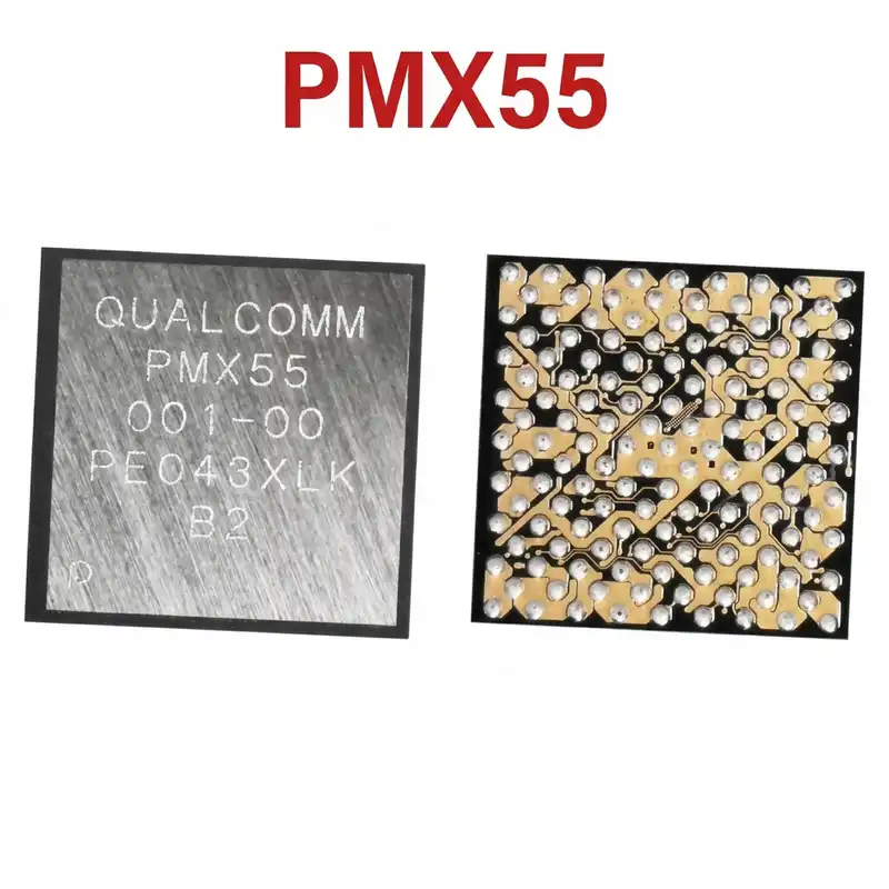
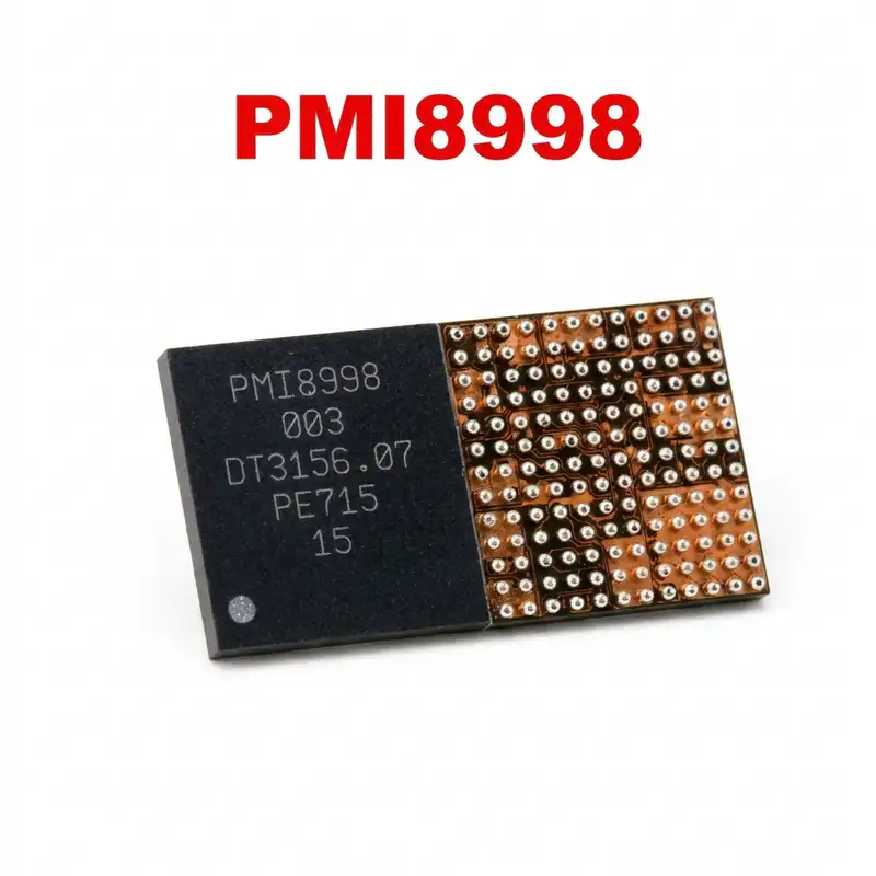
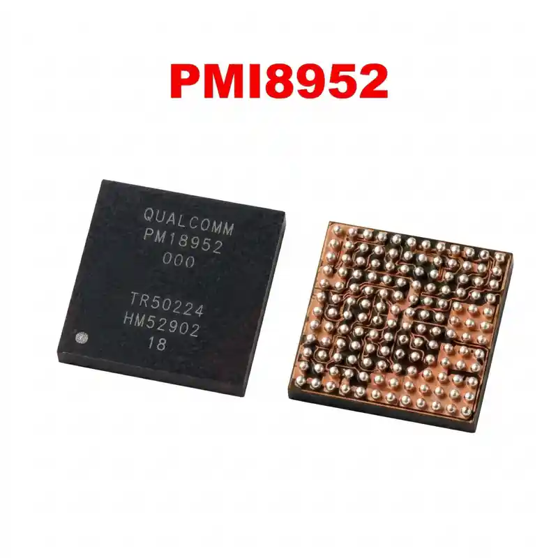
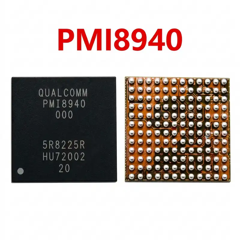
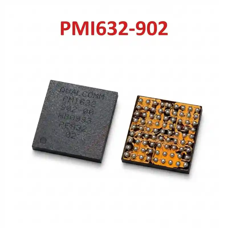
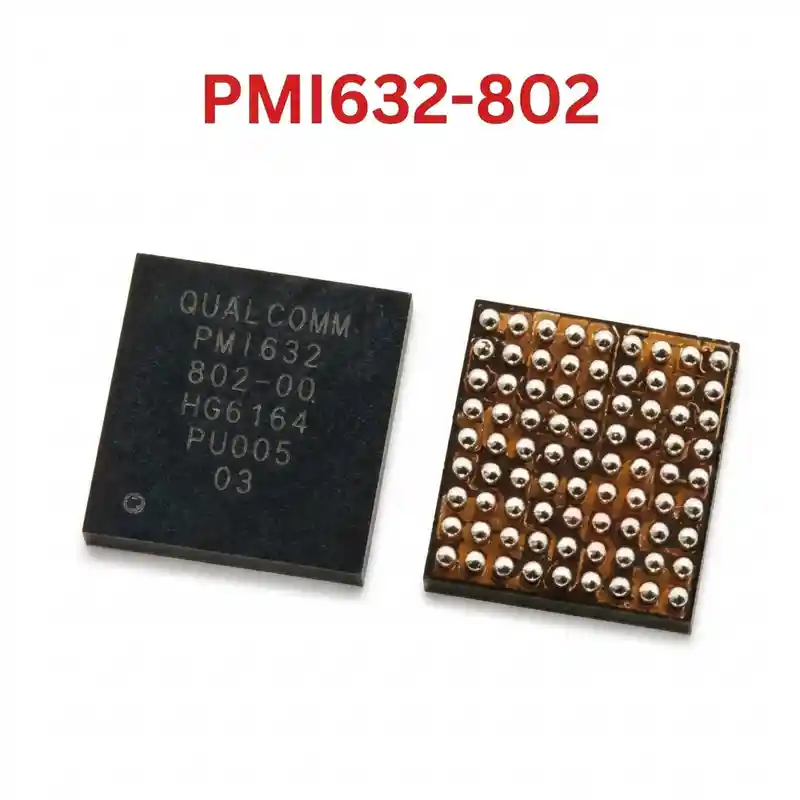
PM6150 IC
As low as
Rs 250.00
Worldwide shipping · Cash on Delivery
Product Details
====================================================================================================
QUALCOMM PM6150-002 PRIMARY SYSTEM PMIC COMPREHENSIVE REPAIR GUIDE
====================================================================================================
1. PRODUCT IDENTIFICATION & HARDWARE SPECIFICATIONS:
----------------------------------------------------------------------------------------------------
- Part Number: PM6150-002 (Laser package silkscreen marking: PM6150 / 002)
- Related Cross-Revisions: PM6150-001, PM6150-102 (Family: Qualcomm PM6150)
- Silicon Manufacturer: Qualcomm Technologies, Inc.
- Platform Architectures: Qualcomm Snapdragon 675 (SM6150), Snapdragon 712, Snapdragon 730
- Multi-PMIC Power Topology: Primary Master PMIC (Paired directly with Secondary Sub-PMIC: PM6150L)
- Functional Classification: Multi-Phase Buck Converter & Precision Multi-Channel LDO PMIC
- Package Configuration: Fine-Pitch Wafer-Level BGA (Ball Grid Array)
- Input Voltage Range: VPH_PWR (3.4V to 4.35V DC) supplied via PM6150L switching node
- Regulated Output Rails:
* Synchronous Step-Down Buck Regulators:
- VDD_APC0 (Kryo 460 Silver Power Efficiency Cluster): ~0.65V – 0.95V Dynamic Voltage Scaling (DVS)
- VDD_APC1 (Kryo 460 Gold High-Performance Cluster): ~0.75V – 1.15V Dynamic Voltage Scaling (DVS)
- VDD_MEM (LPDDR4 / LPDDR4X SDRAM): ~1.125V / 0.6V VDDQ clean supply
- VDD_CORE (Digital Modem Baseband & System Bus): ~0.75V – 0.90V
* 25+ Low-Dropout (LDO) Regulators:
- Dedicated clean supplies for UFS 2.1 / eMMC 5.1 storage (2.95V / 1.8V), System I/O (1.8V VIO),
Camera analog sensors (AVDD 2.8V), and RF transceiver SDR660 PLL supplies.
- Thermal & Soldering Guidelines:
* Reballing Stencil: Amaoe Qualcomm SM6150 / PM6150 Dedicated Stencil (0.12mm)
* Recommended Solder Alloy: 183°C Leaded Solder Paste (Sn63/Pb37)
* Hot Air Rework Settings: 315°C – 325°C (Airflow: 40% – 50%)
2. CIRCUIT ARCHITECTURE & DUAL-PMIC SYNERGY:
----------------------------------------------------------------------------------------------------
- Dual-PMIC Functional Division:
* PM6150-002 (Master PMIC): Exclusively powers application processor CPU/GPU cores, LPDDR4X memory,
38.4MHz base sleep clock (XO), system reset sequencing (PON_RESET_N), and monitors PS_HOLD (1.8V).
* PM6150L (Secondary PMIC): Frontline gateway handling USB Type-C charging, Quick Charge, battery fuel
gauging, LCD backlight boost converter, display bias voltages (+5V/-5V), and camera flash.
- System Handshake & Communications:
* Communicates with the Snapdragon application processor over the SPMI serial bus.
* Senses PWR_KEY ground pulse, initiates internal state machine sequence, enables 38.4MHz crystal,
and awaits 1.8V PS_HOLD acknowledgment from the CPU.
- Target Compatible Smartphones:
* Xiaomi / Redmi: Redmi Note 7 Pro (Violet)
* Samsung: Galaxy A70 (SM-A705), Galaxy A60 (SM-A6060)
* Vivo: Vivo V15 Pro, Vivo V17 Pro, Vivo X27
* Motorola: Moto One Hyper.
3. COMMON MOTHERBOARD FAULT SYMPTOMS:
----------------------------------------------------------------------------------------------------
- Completely Dead Phone (0.00A Current Draw on DC Power Supply):
* Power button triggers no response; missing 1.8V PWR_KEY voltage, defective 38.4MHz crystal, or
fractured BGA solder balls under PM6150-002 caused by drop impact.
- Low Current Stuck / Freezing (0.04A – 0.08A Draw):
* Motherboard draws ~50mA to 80mA upon pressing power key and hangs indefinitely without boot
progression (indicates missing core rail, broken PS_HOLD line, or memory power failure).
- Automatic Qualcomm HS-USB QDLoader 9008 Mode:
* Device connects to PC exclusively in emergency download mode (EDL 9008) with a black screen due to
unstable or missing UFS storage power rails generated by PM6150.
- Restart at Brand Logo / Boot Loop under Load:
* Handset boots up to the startup animation and suddenly restarts as soon as CPU clock speeds spike,
caused by degraded buck output inductors or cracked solder joints on APC core voltage rails.
- Primary VPH_PWR Short Circuit:
* Internal breakdown of PM6150's high-side buck MOSFET pulls the main 4.0V VPH_PWR line to 0V ground.
4. STEP-BY-STEP DIAGNOSTIC & TROUBLESHOOTING:
----------------------------------------------------------------------------------------------------
A. Cold Testing (Multimeter Diode Mode Check):
1. Disconnect battery and Type-C cable completely.
2. Select Diode Mode on digital multimeter. Connect RED probe to motherboard GND shield:
- Main VPH_PWR Input Capacitors: Normal reading is 360mV – 480mV.
- VDD_APC0 / APC1 Buck Coils (CPU Cores): Normal reading 60mV – 120mV (naturally low impedance).
- VDD_MEM Buck Coil (LPDDR4X Memory): Normal reading 260mV – 380mV.
- VDD_CORE Buck Coil: Normal reading 180mV – 280mV.
- 1.8V VIO Peripheral LDO Caps: Normal reading 380mV – 500mV.
3. Diagnostic Rule: A reading of 0.000V indicates a dead short. If found on APC or MEM, isolate
whether the short is inside PM6150 or the CPU using low-voltage DC injection (0.9V – 1.0V)
and thermal imaging or rosin vapor.
B. Hot Testing (Live Operating Voltage Verification):
1. Connect stabilized bench DC power supply at 4.0V to battery terminals.
2. Measure VPH_PWR on filter capacitors surrounding PM6150: Must measure solid 4.0V DC.
3. Check Power Key contact: Must read steady 1.8V DC.
4. Press Power Key and measure voltage on all surrounding buck inductors:
- VDD_APC0 must output 0.75V – 0.90V.
- VDD_MEM must output 1.125V.
- VDD_CORE must output 0.80V.
5. Verify PS_HOLD test point: Must rise from 0V to 1.8V and stay locked high. If PS_HOLD drops back
to 0V after 1–2 seconds, inspect the CPU/RAM combo and UFS storage chip.
5. REWORK, REBALLING & INSTALLATION GUIDELINES:
----------------------------------------------------------------------------------------------------
- Thermal Shielding & Precautions:
* Protect the adjacent Snapdragon CPU and UFS memory chips with polyimide (Kapton) tape and thick
aluminum thermal foil to prevent heat damage or solder ball bridging.
- Chip Desoldering (Removal):
* Apply premium non-corrosive tacky BGA flux around PM6150.
* Set hot air station to 320°C with 45% airflow.
* Move nozzle in smooth concentric circles. As soon as all solder balls liquefy, lift the IC vertically
with precision micro-tweezers. Never force or pry the chip to avoid lifting delicate PCB pads.
- PCB Pad Dressing & Cleaning:
* Flatten solder pads using copper desoldering wick and a chisel-tip soldering iron set to 300°C.
* Clean thoroughly with 99% Isopropyl Alcohol (IPA) and verify under microscope for missing or bridged pads.
- Reballing & Installation:
* Mount PM6150 into a 0.12mm dedicated stencil and apply 183°C leaded solder paste.
* Heat gently at 290°C – 300°C until perfect, uniform solder spheres form.
* Apply a microscope-thin film of flux to motherboard pads, align Pin 1 corner indicator dot with the
silkscreen indicator, and reflow at 310°C until the IC self-aligns. Allow the board to cool naturally.
====================================================================================================
You may also like