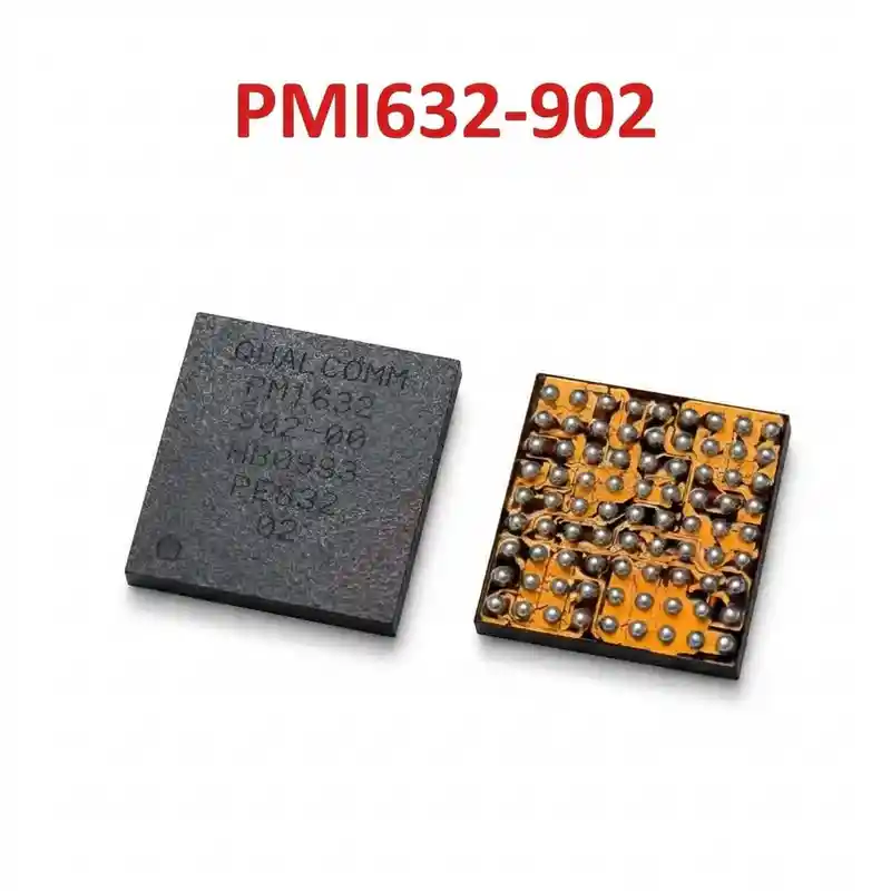
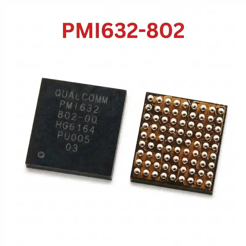
PM439 IC
As low as
Rs 200.00
Worldwide shipping · Cash on Delivery
Product Details
====================================================================================================
QUALCOMM PM439 (PM439-0VV) PRIMARY SYSTEM POWER MANAGEMENT IC GUIDE
====================================================================================================
1. PRODUCT IDENTIFICATION & HARDWARE SPECIFICATIONS:
----------------------------------------------------------------------------------------------------
- Part Number: PM439 (Silkscreen laser markings: "PM439" / "PM439-0VV")
- Alternate Marking: PMI439-0VV / PM-439
- Silicon Manufacturer: Qualcomm Technologies, Inc.
- Chipset Pairing: Qualcomm Snapdragon 439 (SDM439) & Snapdragon 429 Mobile Platforms
- IC Classification: Master System Power Management IC (Primary PMIC)
- Package Type: Fine-Pitch BGA (Ball Grid Array)
- Input Supply Line: VPH_PWR / VBAT rail (Operating range: 3.4V to 4.35V DC)
- Integrated Output Regulators:
* 4x High-Efficiency Synchronous Buck Regulators:
- VREG_S1 (VDD_DIG Core): ~0.8V – 0.95V (Supplies internal digital processing core)
- VREG_S2 (VDD_MEM): ~1.2V (Supplies LPDDR3 / LPDDR4X SDRAM memory)
- VREG_S3 (VDD_APC): ~0.9V – 1.15V (High-current dynamic CPU core supply)
- VREG_S4 (VDD_MODEM): ~1.1V – 1.25V (Baseband modem processing block)
* 20+ Low-Dropout (LDO) Regulators:
- VREG_L5 / L6 (IO): 1.8V (Digital bus, pull-up resistors, sensor I2C lines)
- VREG_L17 / L18 (Analog): 2.8V / 2.85V (Camera analog core, touch controller, biometrics)
- VREG_L19 / L20 (eMMC/UFS): 2.95V – 3.0V (Flash storage VCC rail)
- Stencil Compatibility: Amaoe Universal Qualcomm PMIC / PM439 Stencil (0.12mm)
- Recommended Solder Paste: 183°C Leaded Solder Paste (Sn63/Pb37)
- Hot Air Rework Settings: 315°C – 330°C (Airflow: 40% – 50%)
2. CIRCUIT ARCHITECTURE & STEP-BY-STEP BOOT SEQUENCING:
----------------------------------------------------------------------------------------------------
Stage 1 - Cold Standby State:
- Battery/VPH_PWR (3.8V - 4.2V) enters PM439 input balls.
- PM439 internally generates 1.8V pull-up on the Power Key line (PWR_KEY_N).
Stage 2 - Power-On Trigger:
- Power button is pressed, pulling PWR_KEY_N line to ground (0V).
- PM439 internal state machine wakes up; 38.4MHz crystal oscillator (XO) starts ticking.
Stage 3 - Buck Regulators Activation:
- VREG_S1 (Core), VREG_S2 (RAM), and VREG_S3 (CPU) step-down buck regulators fire sequentially.
Stage 4 - LDO Rails Activation:
- Once Buck rails stabilize, LDO rails (1.8V VIO, 2.95V eMMC, 2.8V Analog) power on.
Stage 5 - System Release & CPU Handshake:
- PM439 releases PON_RESET_N (rises from 0V to 1.8V).
- Main CPU begins executing bootloader code and returns PS_HOLD (1.8V) back to PM439.
- When PS_HOLD is held high, power is locked permanently in the operational awake state.
3. COMPATIBLE SMARTPHONE MODELS:
----------------------------------------------------------------------------------------------------
- Xiaomi / Redmi: Redmi 8, Redmi 8A, Redmi 7A
- Vivo: Vivo Y91, Vivo Y93, Vivo Y95, Vivo Y73
- Samsung Galaxy: Galaxy A01 (SM-A015F/G/DS), Galaxy M01 (SM-M015F)
- Nokia: Nokia 4.2 and various Qualcomm SDM439 platform smartphones.
4. COMMON MOTHERBOARD FAULT SYMPTOMS:
----------------------------------------------------------------------------------------------------
- Complete Dead Phone (0.00A Draw on Power Key): Handset shows no sign of life; pressing the power
key produces zero current draw on a DC power supply (often due to missing 1.8V pull-up on PWR_KEY).
- Stuck Current Draw (0.02A – 0.08A Hanging): When pressing the power key, the current rises to
around 20mA–80mA and stays fixed without fluctuating (indicates missing secondary LDO or no XO clock).
- Qualcomm HS-USB QDLoader 9008 Mode: The device connects directly to PC in 9008 emergency port
without screen display, caused by missing eMMC/RAM supply rails (VREG_L19 or VREG_S2).
- Continuous Boot Loop / Restart at Brand Logo: VREG_S3 (CPU core buck coil) experiences severe voltage
drop under load due to cracked solder balls under PM439 or a degraded buck inductor.
- Primary VPH_PWR Short Circuit (0Ω to GND): Internal high-side switching FET short punctures,
grounding the entire battery line.
5. STEP-BY-STEP DIAGNOSTIC & TESTING PROCEDURES:
----------------------------------------------------------------------------------------------------
A. Cold Testing (Multimeter Diode Mode):
1. Disconnect battery and USB cable completely.
2. Set digital multimeter to Diode Mode.
3. Place RED probe on motherboard ground shield (GND). Probe all surrounding main buck coils:
- VREG_S1 (Core): Normal reading is 180mV – 320mV.
- VREG_S2 (RAM): Normal reading is 300mV – 450mV.
- VREG_S3 (CPU): Normal reading is 120mV – 250mV (naturally low resistance core).
- VREG_S4 (Modem): Normal reading is 320mV – 480mV.
4. Diagnostic Rule: If any coil reads 000mV (dead short), remove the coil or inject 1.0V to
verify if the CPU or PM439 is shorted.
B. Hot Testing (Live Voltage Measurement):
1. Connect DC power supply at 4.0V to the battery terminal.
2. Measure VPH_PWR line around PM439: Must read full 4.0V.
3. Check Power Key voltage: Must read 1.8V DC.
4. Press Power Key and measure all 4 buck coils simultaneously:
- S1 (0.8V), S2 (1.2V), S3 (0.9V - 1.1V), S4 (1.2V) must all rise instantly.
5. Check PS_HOLD test point: Must rise from 0V to 1.8V. If PS_HOLD drops back to 0V, the CPU
has rejected initialization (check eMMC/UFS health or CPU soldering).
6. REWORK, REBALLING & INSTALLATION GUIDELINES:
----------------------------------------------------------------------------------------------------
- Thermal Protection & Masking:
* Mask the CPU/RAM combo and eMMC flash with heat-resistant polyimide thermal tape to prevent
underfilled ICs from blistering or pop-corning.
- Chip Desoldering (Removal):
* Apply premium low-solid tacky BGA flux around the IC perimeter.
* Set hot air station to 320°C with 45% airflow.
* Heat in circular motions until all balls melt; lift vertically using fine tweezers.
- PCB Pad Preparation:
* Clean the motherboard BGA pads flat using a soldering iron (300°C) and copper desoldering wick.
* Clean thoroughly with 99% Isopropyl Alcohol (IPA); check that no pads are bridged or torn under microscope.
- Reballing & Installation:
* Use a 0.12mm dedicated Qualcomm PMIC stencil and 183°C leaded solder paste.
* Form uniform solder spheres at 290°C.
* Apply a microscope-thin layer of flux on the PCB pads. Align Pin 1 index dot precisely.
* Apply hot air at 310°C until the solder balls melt and surface tension pulls PM439 into perfect
alignment (self-centering). Allow the PCB to cool completely before powering on.
====================================================================================================
You may also like