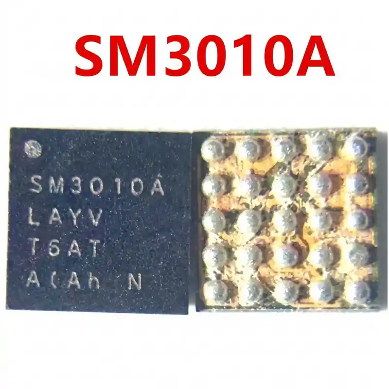
SPU15R IC
As low as
Rs 1000.00
Worldwide shipping · Cash on Delivery
Product Details
====================================================================================================
SAMSUNG SPU15R DETAILED TECHNICAL GUIDE, USAGE & HARDWARE REWORK
====================================================================================================
1. FUNCTIONAL ARCHITECTURE & BOARD WORKING PRINCIPLE:
----------------------------------------------------------------------------------------------------
- Modern Multi-Phase PMIC Architecture:
* The SPU15R is an advanced, high-density power management IC engineered for modern Samsung Exynos
processors (such as Exynos 1330, Exynos 1380, and Exynos 2400e) and Google Tensor platforms.
* It integrates multiple synchronous step-down (buck) converters capable of delivering high-current,
low-ripple power rails to CPU big/LITTLE cores, GPU, NPU, and LPDDR5/LPDDR4X memory.
- Integrated Multi-Channel Low-Noise LDO Regulators:
* Features over 20 ultra-low-noise linear dropout regulators powering optical image stabilization (OIS),
high-resolution camera sensors (VDDA/VDDD), AMOLED display bias rails, and touchscreen digitizers.
- Dynamic Voltage and Frequency Scaling (DVFS):
* Works in real-time coordination with the SoC over high-speed SPMI/I2C buses to adjust core voltages
instantaneously based on processing load, maximizing battery endurance and thermal efficiency.
- Power Sequencing & Reset Controller:
* Manages the strict power-up and power-down timing sequences required by modern 5nm/4nm application
processors, monitoring reset signals and power-good indicators.
2. COMPATIBLE SMARTPHONE PLATFORMS:
----------------------------------------------------------------------------------------------------
- Samsung Galaxy Series:
* Galaxy S24 FE (SM-S721B / SM-S721U)
* Galaxy A54 5G (SM-A546B, SM-A546U, SM-A5460)
* Galaxy A25 5G (SM-A256B, SM-A256E)
* Galaxy A14 5G (SM-A146B, SM-A146P - Exynos 1330 edition)
* Galaxy M14 5G (SM-M146B)
- Google Pixel Series (Samsung-Fabricated Tensor Architecture):
* Google Pixel 7 / Pixel 7 Pro (Tensor G2 companion power rail)
* Google Pixel 8 / Pixel 8 Pro (Tensor G3 auxiliary PMIC tier)
3. BOARD-LEVEL FAULT SYMPTOMS:
----------------------------------------------------------------------------------------------------
- Completely Dead Phone (0.00A – 0.04A Low-Current Freeze on DC Power Supply):
* When SPU15R fails, essential CPU/Memory buck rails are absent; the device cannot initiate boot sequence.
- Boot Loop at First Samsung / Galaxy Logo:
* Device powers on, displays the initial logo, and immediately restarts or shuts down due to missing
secondary LDO output or failure of internal power-good handshake.
- Fake Charging / Battery Discharge While Plugged In:
* Charging icon appears, but battery percentage steadily drops due to internal power-path regulator failure.
- Camera Subsystem Failure ("Camera Failed / Warning"):
* Opening the camera app causes the phone to freeze or exit with a warning error because the camera
analog LDO rails generated by SPU15R are missing or shorted.
- Primary Line Short Circuit (V_SYS / V_BAT Short to GND):
* Punctured high-side buck MOSFET bridges the battery bus directly to ground (0.000V in diode mode).
4. STEP-BY-STEP MULTIMETER TESTING & DIAGNOSTICS:
----------------------------------------------------------------------------------------------------
A. Cold Testing (Diode Mode Check - Board Powered Off, Battery Disconnected):
1. Connect Multimeter RED probe to PCB Ground (GND shield), probe with BLACK probe:
- Main Input Bypass Capacitors around SPU15R: Normal ~360mV – 460mV (0.000V = dead short).
- Processor Core Buck Inductors: Normal ~50mV – 120mV (low impedance is normal, must NOT read 0.000V).
- Memory Rail Inductors: Normal ~200mV – 320mV.
- Peripheral LDO Filter Capacitors: Normal ~420mV – 580mV.
- SPMI / I2C Bus Lines: Normal ~450mV – 550mV (balanced on both clock and data lines).
2. Short-Circuit Thermal Detection:
- If an input line reads 0.000V, inject 3.8V DC (limited to 1.8A).
Inspect with thermal camera: if SPU15R glows white-hot immediately, desolder the IC.
B. Live Operating Voltage Check (Hot Testing):
1. Power up the board via DC bench power supply:
- Check main switching inductors around SPU15R immediately after pressing power button:
* CPU Core Rails: Must output 0.75V – 0.95V DC.
* Memory Rail: Must measure steady 1.10V – 1.20V DC.
* System 1.8V Always-On Line: Must measure rock-solid 1.80V DC.
- If rails briefly pulse once and collapse to 0V, verify whether an external LDO line is shorted
before replacing SPU15R.
5. SOLDERING, REBALLING & REWORK SPECIFICATIONS:
----------------------------------------------------------------------------------------------------
- High-Density BGA Construction (200+ Balls):
* SPU15R features an extremely fine-pitch ball grid array; pad spacing is narrow and prone to bridging
if excess flux or excessive solder paste is applied.
- Surrounding Component Thermal Protection:
* Positioned near the main Exynos processor and UFS 3.1 storage chip.
* Always shield neighboring CPU and UFS flash with thick Kapton thermal tape and copper coins.
- IC Removal:
* Dispense high-grade non-corrosive RMA BGA tacky flux around the perimeter of SPU15R.
* Hot air rework parameters: 320°C – 335°C, airflow 35% – 40% with a medium precision nozzle.
* Heat evenly in circular motions for 30–40 seconds. Once all solder balls liquefy, lift chip vertically.
- PCB Pad Cleanup:
* Apply 183°C (Sn63/Pb37) leaded solder alloy to lower pad alloy melting threshold.
* Flatten pad matrix completely using fine copper desoldering braid with soldering iron set to 285°C – 295°C.
* Clean residue with 99% Isopropyl Alcohol (IPA); inspect all pads under high microscope magnification.
- Reballing Procedure:
* Use a dedicated 0.12mm SPU15 / SPU15R BGA stencil or high-precision universal Samsung PMIC stencil.
* Spread 183°C leaded solder paste smoothly across all apertures with a flexible scraper.
* Reflow gently at 270°C – 280°C with low airflow (20%) until uniform solder spheres form.
- Alignment & Installation:
* Spread a micro-thin layer of tacky BGA flux onto PCB pads.
* Align Pin 1 dot on SPU15R with motherboard silkscreen orientation marking.
* Reflow at 305°C – 315°C with 35% airflow; watch chip gently pull into center via solder surface tension.
* Allow logic board to cool naturally for 3–5 minutes before connecting DC power or battery.
====================================================================================================
You may also like