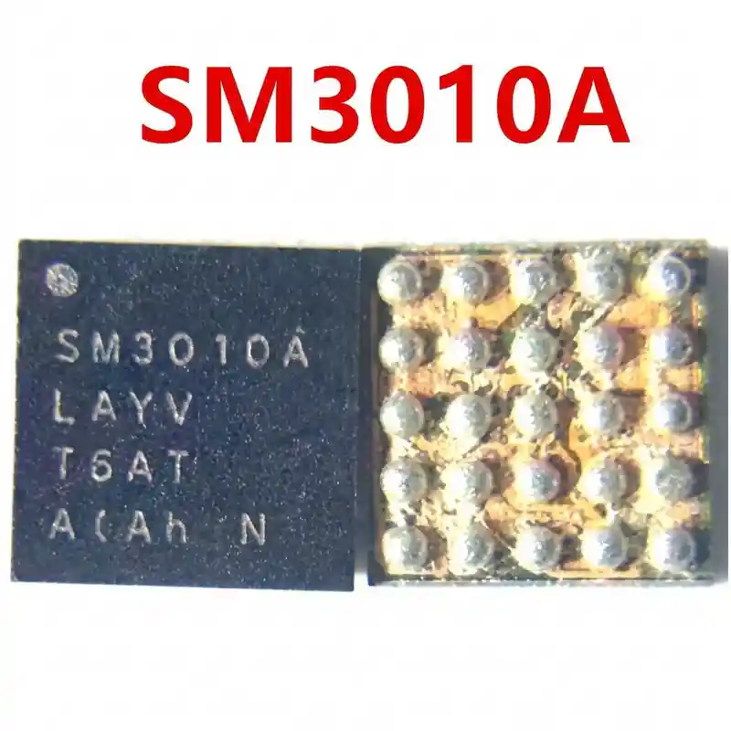
SN2806 IC
As low as
Rs 1000.00
Worldwide shipping · Cash on Delivery
Product Details
====================================================================================================
TEXAS INSTRUMENTS SN2806 / SN2806RGER DETAILED TECHNICAL & REWORK GUIDE
====================================================================================================
1. FUNCTIONAL ARCHITECTURE & BOARD WORKING PRINCIPLE:
----------------------------------------------------------------------------------------------------
- Synchronous Step-Down (Buck) Conversion:
* The SN2806 is an integrated high-efficiency DC-DC synchronous buck regulator designed by Texas
Instruments for compact, thermally constrained mobile and communication logic boards.
* It integrates low Rds(on) high-side and low-side power MOSFETs to convert primary bus voltages
(3.3V – 5.5V DC) into tightly regulated core and auxiliary voltage rails (0.8V to 3.3V DC) with
current capabilities up to 2A–3A.
- High Switching Frequency & Low Ripple:
* Operates at high switching frequencies (1.5MHz to 2.25MHz), allowing the use of miniature external
chip inductors and ceramic output capacitors, saving board space and minimizing output ripple.
- Thermal Dissipation Architecture:
* Encapsulated in a 24-pin QFN (RGE) package featuring a large exposed bottom thermal pad (PowerPAD)
soldered directly to motherboard ground planes to dissipate heat away from the silicon die.
- Protection Circuits:
* Cycle-by-cycle over-current protection (OCP), input under-voltage lockout (UVLO), output over-voltage
protection (OVP), and thermal shutdown with automatic recovery.
2. APPLICATION & BOARD PLACEMENT:
----------------------------------------------------------------------------------------------------
- Primary Circuit Roles:
* Point-of-Load (PoL) DC-DC regulator supplying clean power to baseband processing blocks, memory buses,
or RF transceiver auxiliary rails.
* Secondary power management stage on multi-rail portable communication boards.
3. BOARD-LEVEL FAULT SYMPTOMS:
----------------------------------------------------------------------------------------------------
- Circuit Subsystem Failure / Device Not Booting:
* Failure of internal switching MOSFETs stops output rail generation; downstream processing or RF circuits
remain completely unpowered, preventing device boot or cellular activation.
- Primary Power Rail Dead Short to Ground:
* High-side MOSFET puncture connects the input supply rail directly to GND through the output inductor,
causing bench DC power supplies to trigger short-circuit protection immediately (0.000V in diode mode).
- Severe Component Overheating:
* Internal gate driver degradation causes abnormal shoot-through current, making SN2806 scorching hot
within seconds of power application.
- Output Voltage Fluctuation or Low Voltage Under Load:
* Feedback circuit failure causes output rail to drop significantly when downstream processors increase
current demand, leading to system crash or reboot.
4. STEP-BY-STEP MULTIMETER TESTING & DIAGNOSTICS:
----------------------------------------------------------------------------------------------------
A. Cold Testing (Diode Mode Check - Board Powered Off, Battery Disconnected):
1. Connect Multimeter RED probe to PCB Ground (GND shield), probe with BLACK probe:
- VIN Input Pins / Bypass Capacitors: Normal ~420mV – 540mV (0.000V = dead short).
- SW (Switch Node) / Output Inductor: Normal ~300mV – 450mV (low impedance to ground is expected,
must NOT read 0.000V).
- VOUT Output Filter Capacitors: Normal ~320mV – 480mV.
- EN (Enable Pin) / Control Lines: Normal ~500mV – 650mV.
2. Short-Circuit Thermal Detection:
- If input reads 0.000V, inject 3.8V DC (limited to 1.5A).
Inspect with thermal camera: if SN2806 illuminates white-hot immediately, desolder the IC.
B. Live Operating Voltage Check (Hot Testing):
1. Power up the logic board via DC power supply:
- Verify VIN pin receives steady 3.8V – 5.0V DC.
- Verify Enable (EN) pin is pulled HIGH (1.8V to 3.3V DC logic high from controller).
- Check output inductor terminal: Must measure steady designated DC output voltage (e.g., 1.2V,
1.8V, or 2.5V depending on board configuration).
- If VIN and EN are present but output inductor measures 0V, replace SN2806.
5. SOLDERING, REBALLING & REWORK SPECIFICATIONS:
----------------------------------------------------------------------------------------------------
- Exposed Center Ground Pad (Thermal Pad Rework):
* The SN2806 package features an exposed thermal pad on the bottom. Proper solder coverage on this pad
is critical for ground connection and thermal dissipation; voiding will cause premature thermal shutdown.
- IC Removal:
* Apply non-corrosive RMA tacky flux around the perimeter of the QFN-24 package.
* Hot air rework parameters: 320°C – 335°C, airflow 35% – 40% with a medium nozzle.
* Heat uniformly for 25–35 seconds. Since center pad solder takes longer to melt than perimeter pins,
gently nudge with tweezers; once fully liquid, lift chip vertically.
- PCB Pad Cleanup:
* Add 183°C (Sn63/Pb37) leaded solder to dilute factory high-melt unleaded alloy.
* Clean perimeter pads and center thermal pad completely flat using copper desoldering braid and
soldering iron set to 290°C – 300°C.
* Clean flux residue thoroughly with 99% Isopropyl Alcohol (IPA); inspect pads under microscope.
- Solder Paste & Stencil Application:
* Use a 0.12mm QFN-24 (0.5mm or 0.4mm pitch) stencil.
* Apply 183°C leaded solder paste. For the center pad, apply a cross-hatch or windowed pattern to prevent
solder balling and excessive height.
- Placement & Installation:
* Apply a micro-thin layer of tacky flux. Align Pin 1 dot with silkscreen marking.
* Reflow at 305°C – 315°C with 35% airflow; observe chip self-center on molten solder surface tension.
* Allow motherboard to cool naturally for 3–5 minutes before applying DC power.
====================================================================================================
You may also like