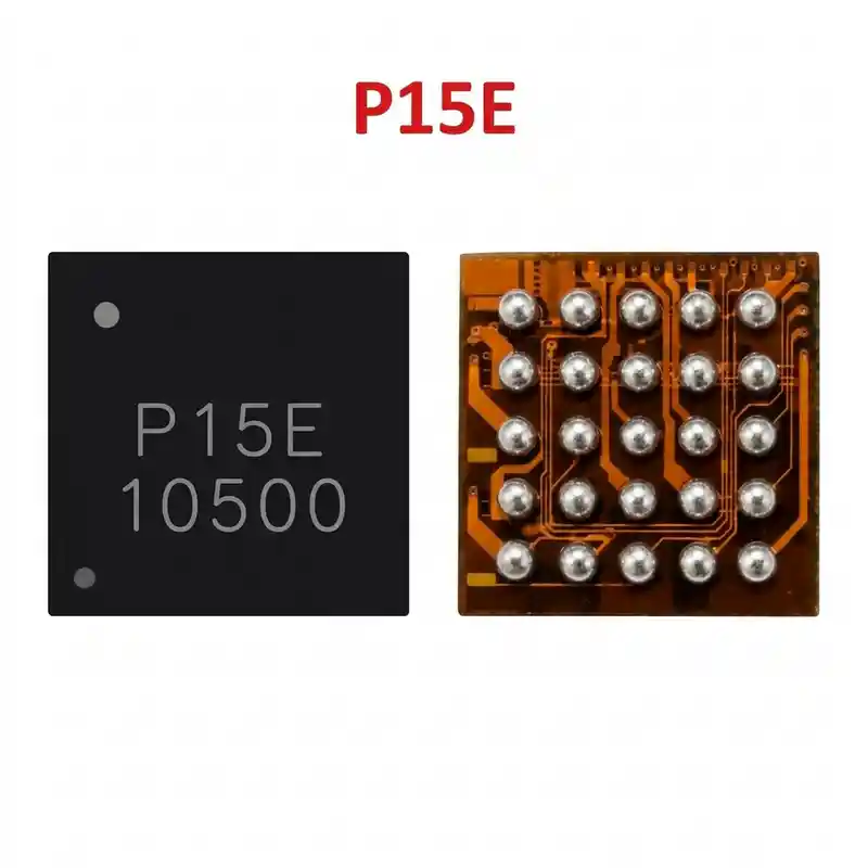
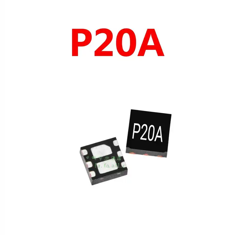
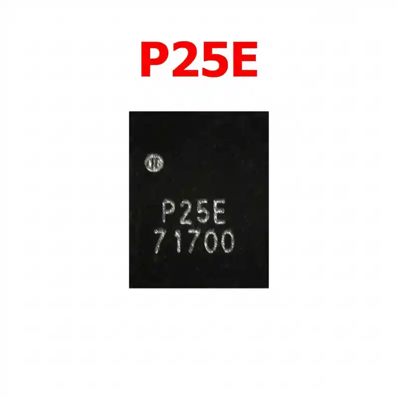
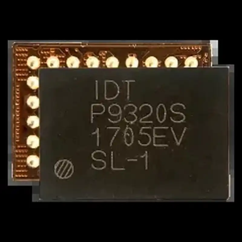
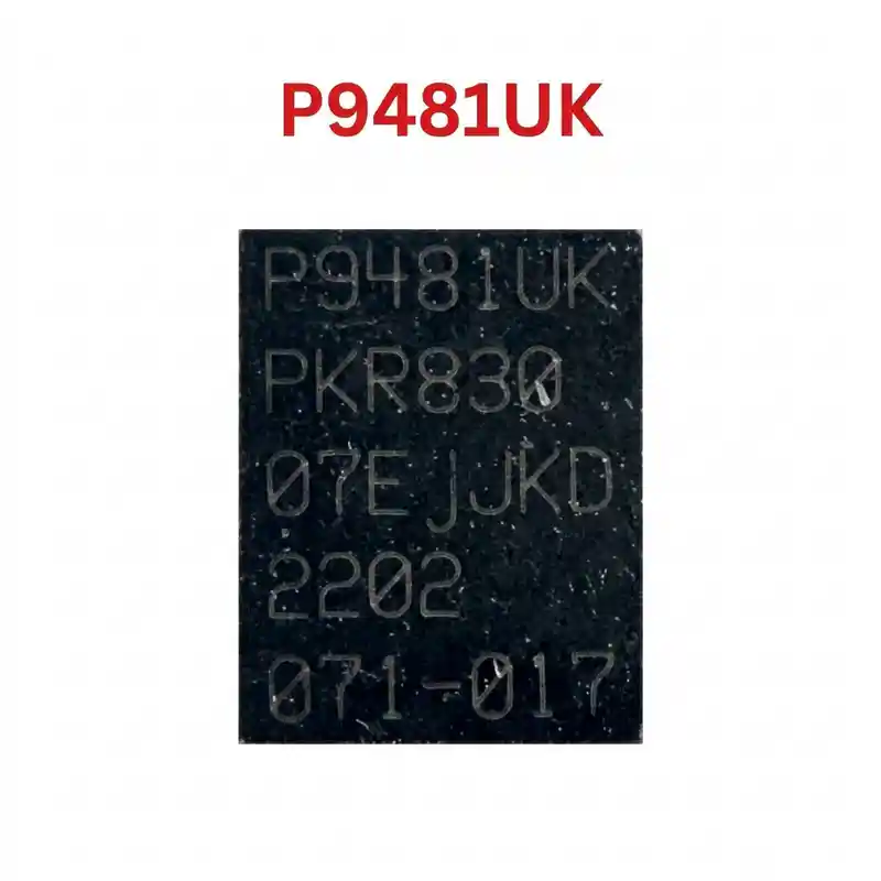
SMB1395 IC
As low as
Rs 300.00
Worldwide shipping · Cash on Delivery
Product Details
====================================================================================================
QUALCOMM SMB1395-001 AUXILIARY CHARGE PUMP IC REWORK & DIAGNOSTIC GUIDE
====================================================================================================
1. FUNCTIONAL ARCHITECTURE & CIRCUIT ROLE:
----------------------------------------------------------------------------------------------------
- Dual-Charge Auxiliary Charge Pump Topology:
* In high-power charging platforms (such as 27W, 30W, and 33W Fast Charging), the main PMIC alone
cannot handle the full charging current without severe thermal throttling.
* SMB1395 functions as a secondary "Charge Pump" (2:1 switched-capacitor voltage divider). It takes
high input voltage from the USB-C adapter (e.g. ~9V–10V) and divides it precisely in half (~4.5V–5V)
while doubling the output current directly to the battery circuit with over 97% efficiency.
- Synchronized Operation with Main PMIC:
* Communicates with the primary Qualcomm PMIC (PM6150 / PM7150) and the Application Processor via
high-speed I2C control buses to dynamically regulate charge current steps and monitor die temperature.
- Independent Over-Voltage & Thermal Protection:
* Features dedicated internal reverse-blocking FETs, input over-voltage protection (OVP), and thermal
monitoring to immediately isolate the charging path if current exceeds safety limits.
2. BOARD-LEVEL FAULT SYMPTOMS:
----------------------------------------------------------------------------------------------------
- Fast Charging Inactive / Throttled to Standard Charging:
* Phone charges normally at 5V / 1.0A–1.5A, but completely fails to trigger "Fast Charge", "Quick Charge",
or "Mi Turbo Charge" when plugged into an original 33W fast charger.
- Charging Cuts Out Under Load:
* The fast charging animation appears for 2 to 3 seconds, then charging disconnects and reconnects
repeatedly in an endless cycle.
- Boot Hang on Company Logo:
* Damage to internal I2C bus registers inside SMB1395 can pull the system communication lines down,
causing the phone to hang permanently on the Redmi / Poco / Samsung boot logo.
- Main VBUS / PMID Short-Circuit:
* Internal FET breakdown shorts the primary VBUS/PMID high-voltage rail directly to ground, causing
the external USB power meter to read 0.000A with zero screen reaction.
- Severe Thermal Runaway:
* SMB1395 becomes burning hot within seconds of connecting a fast-charging Type-C adapter.
3. STEP-BY-STEP MULTIMETER TESTING & DIAGNOSTICS:
----------------------------------------------------------------------------------------------------
A. Cold Testing (Diode Mode Check - Battery & Charger Disconnected):
1. Set digital multimeter to Diode Mode. Place RED probe on motherboard ground (shielding frame)
and use BLACK probe to measure components around SMB1395:
- Flying Capacitors (Charge Pump Switched Capacitors): Measure both sides. Readings must show
balanced diode drop values (~450mV to 650mV). A reading of 0.000V indicates an internal FET failure.
- VBUS / PMID Input Line: Normal reading is ~500mV to 680mV.
- VOUT / Battery Rail Line: Normal reading is ~380mV to 500mV.
- I2C Communication Lines (SDA / SCL): Normal reading is ~480mV to 650mV on both lines.
2. Short Isolation:
- If surrounding filter capacitors measure 0.000V to ground, apply rosin flux or inspect with
a thermal camera while injecting 3.8V DC (limited to 1.5A). If SMB1395 illuminates immediately,
remove the chip from the PCB.
B. Hot Testing (Fast Charger Connected):
1. Connect an original 30W/33W fast charger with a digital USB tester:
- Check input capacitor: Input voltage should rise from 5V to 9V–10V. If voltage stays at 5V,
the IC is failing to handshake QC negotiation.
- Check output flying caps: A steady 4.2V–4.4V high-current output should appear going toward VBAT.
4. SOLDERING, REBALLING & REWORK SPECIFICATIONS:
----------------------------------------------------------------------------------------------------
- Chip Characteristics:
* SMB1395 is a miniature wafer-level chip scale package (WLCSP) with bare silicon top and micro-pitch
solder spheres. It is sensitive to excessive localized heat and physical shearing.
- Desoldering Procedure:
* Protect adjacent components and plastic connectors with Kapton tape or metal heat shields.
* Apply premium non-corrosive RMA tacky flux around the chip.
* Hot air station settings: Temperature 335°C – 345°C, Airflow 30%.
* Heat in even circular motions for 15–20 seconds. Once the solder balls fully melt, gently lift the
chip vertically with fine curved tweezers without sliding across pads.
- PCB Pad Preparation:
* Apply leaded solder paste (Sn63/Pb37, 183°C) to dilute the unleaded factory solder on the PCB pads.
* Wick the pads flat using fine copper desoldering braid and a micro-tip soldering iron at 285°C.
* Clean thoroughly with 99% pure Isopropyl Alcohol (IPA); ensure no solder bridges exist under a microscope.
- Reballing Procedure:
* Use a dedicated SMB1395 / Qualcomm charging BGA stencil (0.12mm thickness).
* Scrape 183°C fine-grain leaded solder paste evenly into all stencil holes.
* Reflow using hot air at 280°C with low airflow (15%–20%) until bright, spherical balls form.
- Placement & Soldering:
* Apply a very thin film of tacky flux on the motherboard footprint.
* Align the Pin 1 orientation index dot with the board silkscreen marking.
* Solder at 310°C with 30% airflow. Allow surface tension to center the IC; gently nudge the corner
to confirm elastic self-alignment.
* Let the board cool down for 5 minutes before connecting the battery and testing charging current.
====================================================================================================