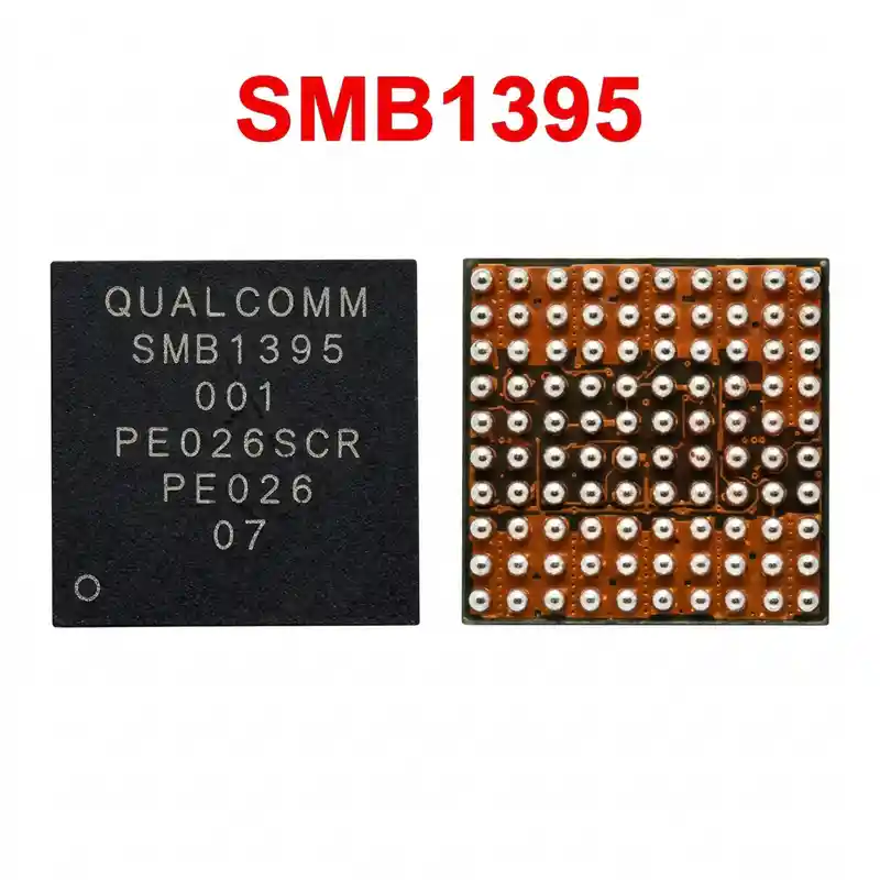
P9481 IC
As low as
Rs 350.00
Worldwide shipping · Cash on Delivery
Product Details
====================================================================================================
P9481UK / P9481-UK SAMSUNG GALAXY S23/S24 SERIES FAST CHARGING IC REPAIR GUIDE
====================================================================================================
1. PRODUCT IDENTIFICATION & SILICON SPECIFICATIONS:
----------------------------------------------------------------------------------------------------
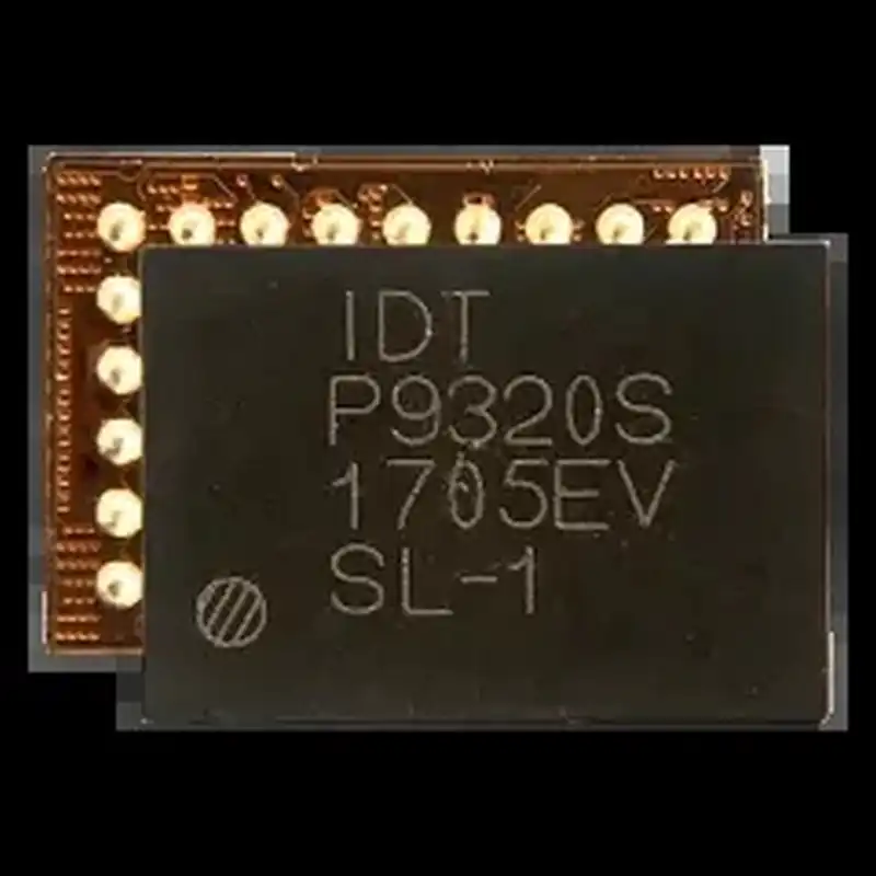
- Silicon Laser Marking: P9481UK (Alternate Code: P9481UX / P9481-UK)
- Component Classification: High-Efficiency Direct Switched-Capacitor Fast Charger & Pump IC
- Target Architecture: Samsung Super Fast Charging 2.0 (45W / 25W USB-PD PPS direct delivery)
- Associated Motherboard Lines: Samsung Galaxy S23 Series & Galaxy S24 Series Logic Boards
- Package Form Factor: 70-Pin High-Density Wafer-Level Chip-Scale BGA (WLCSP / BGA70)
- Functional Circuit Architecture:
* Switched-Capacitor Divider / Multiplier:
- Delivers up to 97.5% efficiency during high-amperage USB-PD PPS fast charging modes.
- 2:1 and 4:1 voltage down-conversion, reducing board heating and thermal throttling by over 60%.
* Input Power-Path & OVP Integration:
- Real-time VBUS voltage monitoring supporting 5V, 9V, 15V, and up to 20V PPS input spikes.
- Integrated ultra-fast Over-Voltage Protection (OVP) isolation switch.
* Autonomous Diagnostic & Sensor Interfacing:
- Continuous real-time measurement of battery current (IBAT) and junction temperature.
- I2C communication bus interfacing directly with the application processor and Sub-PMIC.
2. COMPATIBLE 5G FLAGSHIP SMARTPHONES:
----------------------------------------------------------------------------------------------------
- Samsung Galaxy S23 Series:
* Galaxy S23 5G (SM-S911B, SM-S911U, SM-S911W, SM-S9110)
* Galaxy S23+ 5G (SM-S916B, SM-S916U, SM-S916W, SM-S9160)
* Galaxy S23 Ultra 5G (SM-S918B, SM-S918U, SM-S918W, SM-S9180)
- Samsung Galaxy S24 Series:
* Galaxy S24 5G (SM-S921B, SM-S921U, SM-S9210)
* Galaxy S24+ 5G (SM-S926B, SM-S926U, SM-S9260)
* Galaxy S24 Ultra 5G (SM-S928B, SM-S928U, SM-S9280)
3. TYPICAL BOARD-LEVEL FAULT SYMPTOMS:
----------------------------------------------------------------------------------------------------
- Complete Loss of Fast Charging (Freezes at Standard 5V 0.5A – 1.0A Slow Rate):
* When connected to an original 45W / 25W Samsung Super Fast charger, the phone fails to negotiate
the PPS protocol. The display shows basic slow cable charging without the characteristic cyan/blue ring animation.
- Fake Charging (Charging Animation Present but Battery Percentage Drops):
* Lightning bolt indicator is visible in the status bar, but battery percentage stays fixed or drains
during screen-on usage due to damaged internal charge pump switching FETs.
- "Moisture Detected" or "Charging Paused / Temperature Error":
* System alerts that charging is suspended due to temperature limits or port anomalies, caused by
corrupted analog sense lines inside the P9481UK package following liquid ingress.
- VBUS Input Line Dead Short Circuit (0.000V in Diode Mode):
* Internal gate breakdown inside P9481UK shorts the main USB VBUS power line directly to ground,
causing external chargers to trigger overcurrent shutdown immediately upon insertion.
- Severe Motherboard Overheating During Fast Charge:
* Phone becomes extremely hot around the middle/lower logic board section within 2 minutes of plugging
into a high-wattage charger.
4. STEP-BY-STEP MULTIMETER TESTING & DIAGNOSTICS:
----------------------------------------------------------------------------------------------------
A. Cold Testing (Diode Mode Check - Board Powered Off, Battery & Flex Cables Disconnected):
1. Place digital multimeter in Diode Mode. Connect RED probe to motherboard GND shield:
- VBUS Input Test Points / Filter Capacitors: Normal ~480mV – 620mV.
- VCHG Output Capacitors (Line to Battery FPC): Normal ~380mV – 510mV.
- Flying Capacitor (CFLY) Nodes on P9481UK: Normal ~420mV – 540mV (must be closely balanced).
- I2C Clock & Data Bus Lines (SCL / SDA): Normal ~450mV – 560mV (matched within 10mV).
2. Short-Circuit Isolation:
- If VBUS or VCHG line reads 0.000V (beeping dead short to ground), inject 4.0V DC (current limit 1.5A).
Inspect the P9481UK area using a thermal imaging camera or rosin smoke: if P9481UK illuminates white-hot,
remove the IC to clear the short.
B. Live Operating Voltage Check (Hot Testing):
1. Connect an active USB Type-C 25W/45W PD charger to the phone:
- Verify input voltage across bypass capacitors: Must step up from 5.0V to 9.0V or 15V DC as fast charging engages.
- Measure output capacitor feeding battery path: Must show stable charging voltage (4.0V – 4.35V DC)
with high current delivery.
- If input remains locked at 5.0V and output does not charge, check I2C communication with AP/PMIC.
5. SOLDERING, REBALLING & REWORK SPECIFICATIONS:
----------------------------------------------------------------------------------------------------
- Extreme Thermal Sensitivity (Ultra-Dense Flagship Logic Board):
* P9481UK is a fine-pitch 70-ball BGA component situated on multi-layer high-density PCB substrate.
* Always shield the adjacent main processor, memory stack, and primary PMICs with multi-layer Kapton tape
and thick copper heatsink coins.
- IC Removal:
* Dispense high-purity, non-corrosive RMA tacky BGA flux around the chip perimeter.
* Hot air rework station settings: 315°C – 325°C with 35% – 45% airflow (precision circular nozzle).
* Move nozzle in uniform circles for 30–40 seconds. Once all 70 solder balls liquefy, lift the IC vertically.
- PCB Pad Cleanup:
* Apply 183°C leaded solder to motherboard footprint pads to lower the eutectic melting threshold.
* Level pads perfectly flat using copper desoldering braid and an iron tip set to 290°C – 300°C.
* Clean residual flux thoroughly with 99% Isopropyl Alcohol (IPA); inspect pads under microscope for any lifted traces.
- Reballing Procedure:
* Use a dedicated 0.12mm Amaoe Samsung Galaxy S23/S24 middle-layer / charging IC stencil.
* Squeegee 183°C (Sn63/Pb37) leaded solder paste uniformly into all 70 apertures.
* Reflow gently with hot air at 280°C – 290°C with low airflow (20%) until uniform solder spheres form.
- Alignment & Installation:
* Spread a microscopic, transparent film of BGA flux over PCB pads.
* Align Pin 1 orientation dot precisely with the PCB silkscreen corner indicator.
* Reflow at 305°C – 315°C with 35% airflow until chip self-centers on solder surface tension.
* Allow motherboard to cool naturally to room temperature for at least 5 minutes before connecting DC power or charger.
====================================================================================================