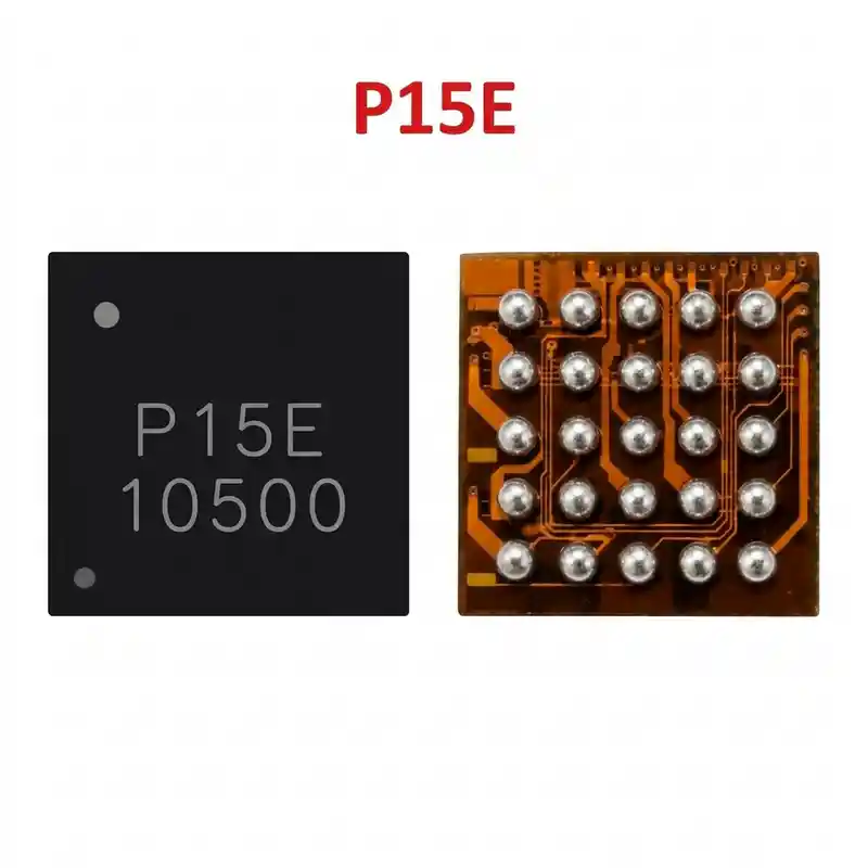
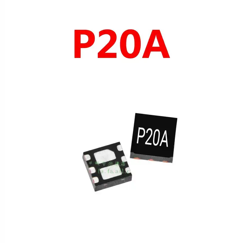
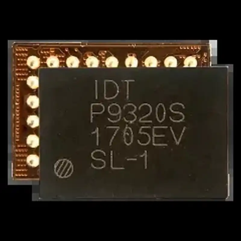
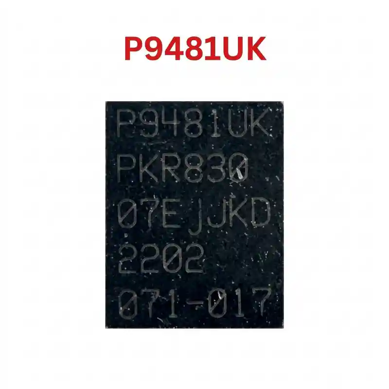
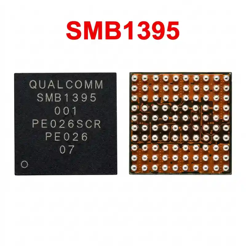
P25E IC
As low as
Rs 200.00
Worldwide shipping · Cash on Delivery
Product Details
====================================================================================================
P25E (P5425 / PSC25) 20-PIN FAST CHARGING & OVP IC
====================================================================================================
1. PRODUCT IDENTIFICATION & HARDWARE SPECIFICATIONS:
----------------------------------------------------------------------------------------------------
- Part Number: P25E
- Common Laser Markings: P25E, P5425, PSC25
- Cross-Compatible Replacements: P15E, P5415A, 6937
- IC Classification: Fast Battery Charging Controller & Over-Voltage Protection (OVP) IC
- Silicon Manufacturer: Samsung Semiconductor / Richtek Technology
- Package Type: 20-Pin SMD / QFN / WLCSP (Flat No-Lead Miniature Package)
- Pin Layout: 20 Pins (4x5 Matrix / Peripheral Leadless Pads)
- Input Voltage Range (VBUS): 4.5V – 6.0V DC (OVP Trigger Limit: ~6.3V)
- Output Voltage (VBAT / VOUT): 3.7V – 4.35V / 4.4V High-Capacity Li-ion Battery Charging Rail
- Continuous Charge Current: 1.5A to 2.0A Maximum Pass-Through
- Reballing Stencil: Amaoe Universal 20-Pin Charging / 0.12mm QFN Stencil
- Recommended Solder Paste: 183°C Leaded Solder Paste (Sn63/Pb37)
- Hot Air Rework Temperature: 305°C – 325°C (Airflow: 40% – 45%)
2. CIRCUIT ARCHITECTURE & MOTHERBOARD ROLE:
----------------------------------------------------------------------------------------------------
- Fast Charge Power Path: Routes and conditions charging current from USB Type-C or Micro-USB ports
directly to the battery terminal and primary PMIC.
- Over-Voltage Protection (OVP): Fast internal power FET disconnects input within microseconds if
external charger voltage exceeds safe limits (>6.3V), guarding downstream logic chips.
- Reverse Current Blocking: Automatically isolates battery voltage from the charging port when the
cable is unplugged to prevent battery leakage.
- Target Devices & Motherboard Applications:
* Samsung Galaxy A-Series: Galaxy A10s, A20, A20s, A30, M10s, M20
* Vivo: Y-Series budget and mid-range devices
* Xiaomi / Redmi: Redmi 8, Redmi 8A, and select entry-level Note series models
* Samsung Galaxy Tab budget motherboards and sub-boards.
3. COMMON MOTHERBOARD FAULT SYMPTOMS:
----------------------------------------------------------------------------------------------------
- Zero Current Draw (0.00A on USB Ammeter): Charger is connected, but the handset draws 0.00A.
Screen remains completely dark with no charging lightning bolt icon.
- Fake Charging: Charging animation runs continuously on the display, but battery percentage does
not increase or gradually drains while plugged in.
- Dead Handset (VBUS Shorted to GND): Damaged by surge or counterfeit 12V vehicle chargers.
Internal switching FET punctures, dropping the entire VBUS 5V line to ground (0Ω).
- Slow Charging (Limited to 0.15A - 0.40A): Internal FET resistance increases due to thermal wear,
causing severe voltage drop (output delivers only 2.5V - 3.2V instead of 4.2V).
- Thermal Runaway / Localized Overheating: Severe heat generation detected around the charging IC
area immediately upon plugging in the charging cable.
4. STEP-BY-STEP DIAGNOSTIC & TESTING PROCEDURES:
----------------------------------------------------------------------------------------------------
A. Cold Testing (Multimeter Diode Mode):
1. Disconnect battery and USB charging cable completely.
2. Set digital multimeter to Diode Mode.
3. Place RED probe on ground (PCB shield / ground pad) and BLACK probe on peripheral test points:
- VBUS Input Filter Capacitor: Normal reading is 480mV – 620mV.
- VBAT Output Filter Capacitor: Normal reading is 360mV – 460mV.
4. Fault Evaluation: If either rail beeps with 000mV – 010mV, P25E is internally shorted to ground
or an adjacent parallel decoupling capacitor is punctured.
B. Hot Testing (Live Voltage Measurement):
1. Connect an active 5V charging cable to the board.
2. Set multimeter to DC 20V range.
3. Measure input capacitor: Confirm 5.0V – 5.2V VBUS is present.
4. Measure output coil/capacitor: Confirm 3.7V – 4.2V VBAT output is generated.
5. Diagnostic Rule: If 5.0V input is verified but output voltage is 0.0V or below 3.0V, P25E is
open/failed and must be replaced.
5. REWORK, REBALLING & INSTALLATION INSTRUCTIONS:
----------------------------------------------------------------------------------------------------
- Thermal Protection & Masking:
* Shield adjacent plastic components (SIM trays, FPC connectors) with high-temperature polyimide
tape or mechanical heat shields.
- Chip Desoldering (Removal):
* Apply a small amount of non-corrosive BGA flux around the IC perimeter.
* Set hot air rework station to 315°C with 40% airflow.
* Direct heat in smooth, circular motions around the package. Lift vertically with fine tweezers
as soon as solder liquifies to avoid tearing delicate PCB pads.
- Board Pad Preparation:
* Apply flux and clean PCB pads using a soldering iron tip (300°C) with copper desoldering braid.
* Clean residue with Isopropyl Alcohol (IPA) and a lint-free swab; verify pad flatness under microscope.
- Reballing & Soldering (Installation):
* Align the 0.12mm universal stencil, apply 183°C leaded solder paste, and scrape flush.
* Melt solder paste under hot air (280°C - 300°C) to form uniform balls.
* Apply a thin layer of flux on motherboard pads. Align Pin 1 dot according to silkscreen marking.
* Heat gently at 305°C until the IC naturally pulls itself into exact alignment (self-centering).
* Allow PCB to cool naturally before reconnecting battery and running functional charge tests.
====================================================================================================