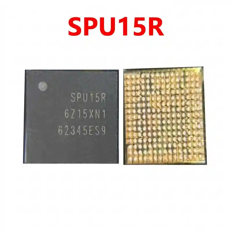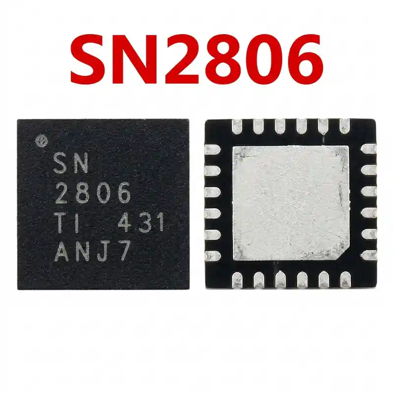

SM5720 IC
As low as
Rs 300.00
Worldwide shipping · Cash on Delivery
Product Details
====================================================================================================
SAMSUNG SM5720 BASEBAND PMIC REWORK & DIAGNOSTIC HARDWARE GUIDE
====================================================================================================
1. FUNCTIONAL ARCHITECTURE & CIRCUIT ROLE:
----------------------------------------------------------------------------------------------------
- Dedicated Baseband Power Generation:
* Operates from the main system voltage rail (VDD_MAIN / VBAT) to generate precise buck voltages for the
cellular baseband processor (Shannon Modem core, I/O, and memory interconnects).
- RF Transceiver & Front-End LDO Supplies:
* Houses integrated low-noise, high-PSRR LDO regulators dedicated to sensitive RF transceivers, mixers,
and power amplifier control logic, preventing baseband digital switching noise from coupling into the RF chain.
- Power State & Sleep Synchronization:
* Communicates with the Application Processor (AP) and Main PMIC (S555) via high-speed control lines to put
the modem into low-power sleep mode during standby and wake it up during incoming/outgoing calls or data bursts.
2. BOARD-LEVEL FAULT SYMPTOMS:
----------------------------------------------------------------------------------------------------
- Unknown Baseband Version / Null IMEI (*#06# Blank):
* In phone Settings > About Phone, the "Baseband Version" displays "Unknown", and dialing *#06# fails to show
the IMEI numbers because the modem processor is completely unpowered or held in reset.
- No Network / Emergency Calls Only / Searching for Service:
* Phone displays "No Service", a circle with a slash (⊘), or searches indefinitely without latching onto
any 2G/3G/4G network carrier.
- Immediate Phone Restart Upon SIM Card Insertion:
* The phone boots normally, but as soon as a SIM card is inserted and the modem powers up, the phone
freezes or restarts immediately (caused by a collapsing buck power rail or short in SM5720).
- High Battery Leakage / Rapid Discharge:
* Phone battery drains in 3 to 5 hours even in airplane mode or standby due to internal quiescent current
leakage (draws 120mA–350mA on DC power supply when asleep).
- Main Power Rail Short-Circuit (Dead Motherboard):
* Internal high-side switching FET breakdown shorts VDD_MAIN / VBAT to ground, causing an instant 0.000V short
that trips the DC power supply before the power button is even pressed.
- Localized Overheating:
* SM5720 becomes scalding hot to the touch within seconds of booting or during network search.
3. STEP-BY-STEP MULTIMETER TESTING & DIAGNOSTICS:
----------------------------------------------------------------------------------------------------
A. Cold Testing (Diode Mode Check - Battery & Charger Disconnected):
1. Set digital multimeter to Diode Mode. Place RED probe on PCB ground (metal shield frame) and probe
components surrounding SM5720 with the BLACK probe:
- Main Input Voltage Rail (VBAT / VDD_MAIN): Normal reading is ~380mV to 520mV (0.000V indicates
a dead primary short).
- Baseband Buck Coils (Surrounding SM5720): Normal readings typically range from ~280mV to 420mV.
- RF Transceiver Power Output Capacitors: Normal readings range from ~450mV to 650mV.
- Baseband Clock & Reset Lines: Normal reading is ~500mV to 700mV.
2. Short-Circuit Verification:
- If any buck coil or power rail shows 0.000V with a continuous multimeter beep, apply rosin smoke
or freeze spray over SM5720 and inject 1.2V–1.8V (limited to 1.5A) into the shorted rail to verify
if SM5720 melts the rosin.
B. Hot Testing (Phone Powered On & SIM Card Inserted):
1. Connect motherboard to a DC bench power supply set to 4.0V:
- Check input capacitor to SM5720: Must show full battery/system voltage (3.8V to 4.0V DC).
- Check baseband output inductors during boot sequence: Must output stable baseband core voltages
(~0.85V to 1.1V DC) and I/O voltages (1.8V DC). If input voltage is present but all output coils
remain at 0V, SM5720 is defective, has cracked solder joints, or lacks the enable signal.
4. SOLDERING, REBALLING & REWORK SPECIFICATIONS:
----------------------------------------------------------------------------------------------------
- BGA Package Handling:
* SM5720 is situated near delicate RF shielding and components. Use adequate shielding to avoid overheating
the baseband processor or nearby RF transceiver chips.
- Desoldering Procedure:
* Cover adjacent plastic SIM tray slots and RF components with double-layer Kapton and aluminum heat shield tape.
* Apply a small amount of high-grade RMA tacky flux around the chip edges.
* Hot air rework parameters: Temperature 330°C – 340°C, Airflow 25%–30%.
* Heat in consistent circular patterns for 15–20 seconds. Once the solder spheres liquefy, lift the chip
straight up using precision micro-tweezers without sliding horizontally.
- Motherboard Pad Cleanup:
* Apply leaded solder paste (Sn63/Pb37, 183°C) to the pads to reduce the melting point of residual lead-free solder.
* Smooth and wick the pads completely flat using fine copper desoldering braid at 280°C.
* Clean thoroughly with 99% pure Isopropyl Alcohol (IPA); inspect under a microscope to confirm no bridged
or lifted copper pads.
- Reballing Procedure:
* Use a dedicated Samsung S8 / Note 8 Baseband / Small PMIC BGA stencil (0.12mm thickness).
* Smooth 183°C leaded solder paste evenly into the stencil apertures.
* Reflow with hot air at 280°C and low airflow (15%) until shiny, uniform spherical balls form.
- Placement & Final Reflow:
* Apply a very light coat of tacky flux over the motherboard pad footprint.
* Align the Pin 1 orientation dot on SM5720 with the silkscreen corner indicator on the PCB.
* Reflow at 305°C – 315°C with 25% airflow. The chip will automatically settle into perfect alignment via
solder surface tension.
* Allow the motherboard to cool naturally for 3 to 5 minutes before testing baseband version and SIM network latch.
====================================================================================================
You may also like