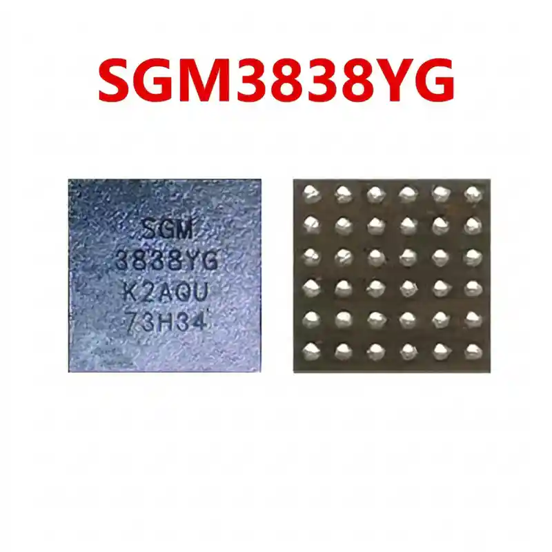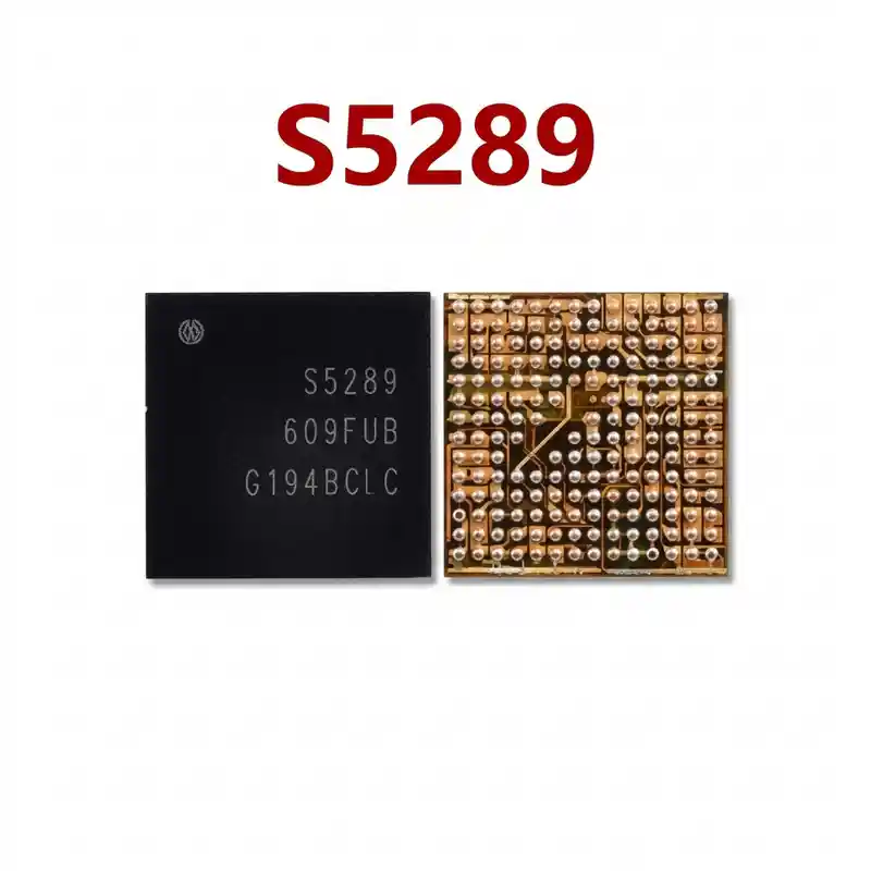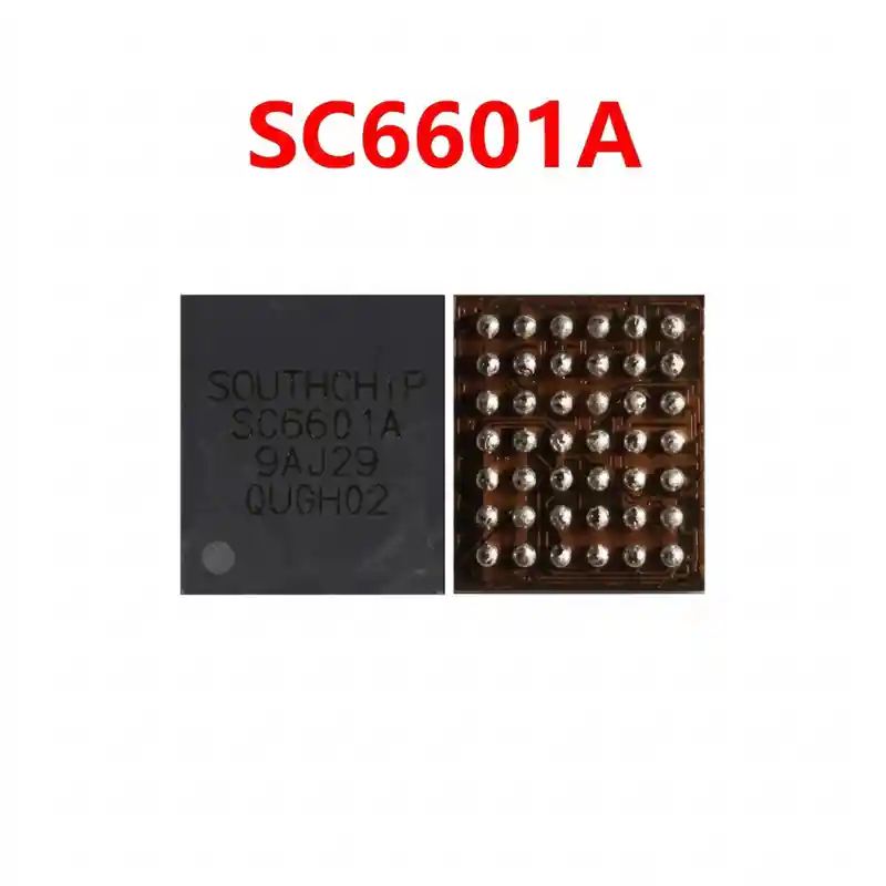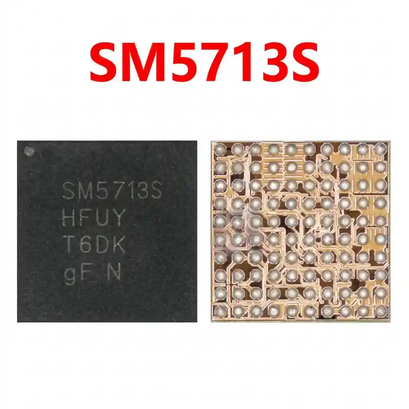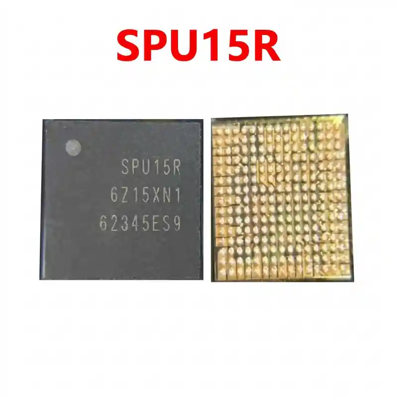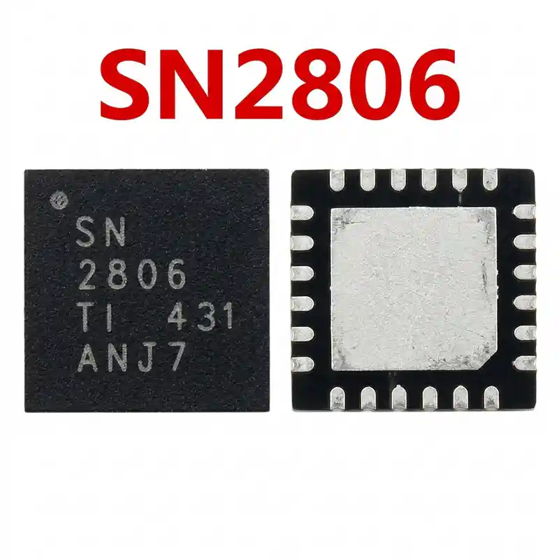

SM5701 IC
As low as
Rs 180.00
Worldwide shipping · Cash on Delivery
Product Details
====================================================================================================
SAMSUNG SM5701 CHARGING & USB IC REWORK & DIAGNOSTIC GUIDE
====================================================================================================
1. FUNCTIONAL ARCHITECTURE & CIRCUIT ROLE:
----------------------------------------------------------------------------------------------------
- Synchronous Switching / Linear Charging Management:
* Receives 5.0V input voltage via VBUS directly from the micro-USB connector.
* Regulates the charging cycle (Pre-charge, Constant Current [CC], Constant Voltage [CV], and Cut-off)
to charge single-cell Li-ion batteries safely up to 4.20V / 4.35V.
- USB DP / DM Data Line Multiplexing:
* Routes differential USB data signals (Data+ / Data-) between the physical connector and the main baseband/AP
processor, managing charger identification (DCP, CDP, SDP) and software flashing / ADB connectivity.
- Power Path & Protection Features:
* Integrated reverse-blocking switch prevents battery discharge back into the charging port.
* Monitors battery pack temperature via the NTC thermistor pin; suspends charging if excessive heat
or cold is detected.
2. BOARD-LEVEL FAULT SYMPTOMS:
----------------------------------------------------------------------------------------------------
- No Charging Reaction (0.00A Current Draw):
* When the charger is plugged in, the phone shows no charging indicator, and a USB power meter displays
0.000A current draw, even with a verified working charging port and battery.
- Fake Charging (Charging Logo Appears but Battery Percentage Drains):
* The screen displays the charging lightning bolt icon, but the USB meter shows minimal draw (0.02A–0.06A).
The battery percentage never increases and gradually drops while plugged in.
- Phone Dead Due to VBUS or VBAT Short-Circuit:
* Internal power MOSFET breakdown causes a complete short to ground (0.000V in diode mode) on VBUS or VBAT,
causing bench power supplies to trip immediately upon connection.
- Computer Does Not Recognize USB (Flashing / Odin / ADB Failure):
* The phone charges when connected to a wall adapter, but Windows PC / Odin tool shows "USB Device Not Recognized"
because internal DP/DM switching transistors inside SM5701 are damaged.
- Temperature Warning Triangle (Yellow Triangle with Thermometer):
* The phone halts charging and displays "Charging paused: Battery temperature too high/low" due to a faulty
internal ADC sensing circuit inside SM5701.
- Excessive Heat Generation:
* SM5701 becomes scalding hot immediately upon inserting the USB charging cable.
3. STEP-BY-STEP MULTIMETER TESTING & DIAGNOSTICS:
----------------------------------------------------------------------------------------------------
A. Cold Testing (Diode Mode Check - Battery & Charger Disconnected):
1. Set digital multimeter to Diode Mode. Place RED probe on PCB ground (metal shield frame) and probe
the components adjacent to SM5701 with the BLACK probe:
- VBUS Input Filter Capacitor (5V Line): Normal reading is ~520mV to 680mV (0.000V indicates
an input short).
- VBAT Output Filter Capacitor: Normal reading is ~380mV to 520mV (matches battery connector terminal).
- USB Data Lines (DP / DM): Normal readings are ~550mV to 720mV on both lines (must be balanced
within 15mV of each other).
- Charging Indicator / Enable Line: Normal reading is ~480mV to 650mV.
2. Short-Circuit Verification:
- If VBUS shows 0.000V, remove the input capacitor first. If the short persists, SM5701 has an
internal high-side FET breakdown and must be replaced.
B. Hot Testing (USB Charger Connected):
1. Connect a 5V USB charger through a USB power doctor meter:
- Measure voltage on the VBUS input capacitor: Must show a stable 5.0V to 5.2V DC.
- Measure voltage on the VBAT output capacitor: Must show active battery charging voltage (3.7V to 4.2V DC).
If VBUS has 5V but VBAT capacitor shows 0V or remains strictly at battery resting voltage without current
draw, SM5701 is defective.
4. SOLDERING, REBALLING & REWORK SPECIFICATIONS:
----------------------------------------------------------------------------------------------------
- 24-Pin WLCSP BGA Package:
* SM5701 is a small wafer-level BGA chip situated close to the battery connector and motherboard edges.
- Desoldering Procedure:
* Shield surrounding plastic components, battery terminal plastic, and microphone with Kapton tape.
* Apply a small amount of non-corrosive RMA tacky flux around the perimeter of the IC.
* Hot air rework parameters: Temperature 320°C – 330°C, Airflow 25%–30%.
* Apply circular heat for 12–15 seconds. Once the solder spheres liquefy, lift the chip vertically
with precision micro-tweezers.
- Motherboard Pad Preparation:
* Apply a small dab of leaded solder paste (Sn63/Pb37, 183°C) to lower the melting temperature of factory solder.
* Flatten and clean the 24 micro-pads using fine copper desoldering braid at 275°C.
* Clean thoroughly with 99% pure Isopropyl Alcohol (IPA); verify under a microscope that no solder bridge exists.
- Reballing Procedure:
* Use a universal charging IC / Samsung J-series BGA stencil (0.12mm thickness).
* Spread 183°C fine-grain leaded solder paste evenly into all 24 apertures.
* Reflow with hot air at 275°C with low airflow (15%) until shiny, uniform spherical balls form.
- Placement & Final Reflow:
* Apply a thin, transparent film of tacky flux onto the motherboard footprint.
* Align the Pin 1 index dot on SM5701 with the silkscreen corner marker on the PCB.
* Reflow at 305°C – 315°C with 25% airflow. The chip will automatically snap into center alignment
via molten solder surface tension.
* Allow the motherboard to cool down for 3 minutes before connecting the charger and testing current draw.
====================================================================================================
You may also like