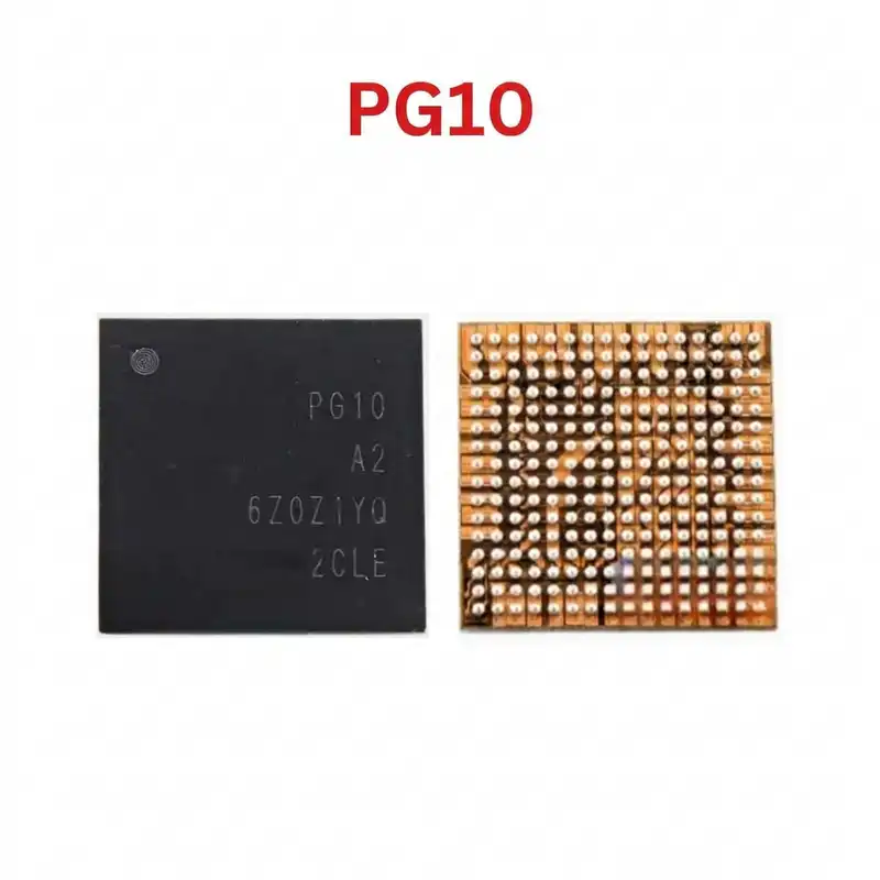
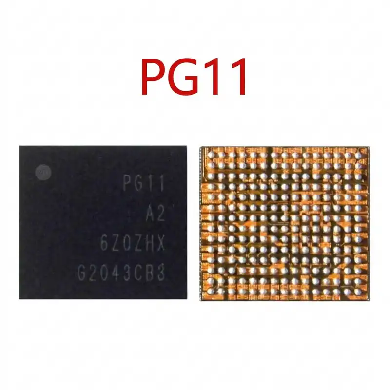
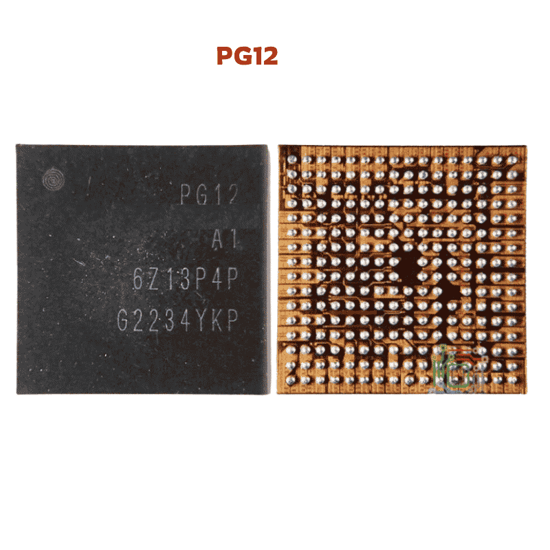
PG13 IC
As low as
Rs 600.00
Worldwide shipping · Cash on Delivery
Product Details
====================================================================================================
PG13 SECONDARY POWER MANAGEMENT & VOLTAGE REGULATOR IC GUIDE
====================================================================================================
1. PRODUCT IDENTIFICATION & HARDWARE SPECIFICATIONS:
----------------------------------------------------------------------------------------------------
- Part Number: PG13 (Top laser silkscreen marking: "PG13")
- IC Product Family: PG-Series Mobile Power & Auxiliary Voltage Regulators
- Silicon Manufacturer: SGMICRO / Mobile Power Management Technology Partners
- IC Classification: Auxiliary PMIC, Camera Subsystem LDO & Multi-Rail Power Regulator
- Package Type: WLCSP / Miniature Micro-BGA (Wafer-Level Chip Scale Package)
- Solder Ball Grid Layout: Ultra-Compact Micro-BGA Footprint
- Input Supply Voltage (VIN): 3.3V – 4.35V DC (Connected directly to system VPH_PWR / VBAT rail)
- Regulated Output Rails: Multi-Channel Outputs: 1.8V (Digital IO), 2.8V / 3.0V (Analog/Sensor)
- Output Current Capacity: 300mA to 600mA per channel with high transient response
- Stencil Compatibility: Amaoe Universal 0.12mm Mobile PMIC / Secondary Power Stencil
- Recommended Solder Paste: 183°C Leaded Solder Paste (Sn63/Pb37)
- Hot Air Rework Settings: 300°C – 320°C (Airflow: 35% – 45%)
2. CIRCUIT ARCHITECTURE & MOTHERBOARD ROLE:
----------------------------------------------------------------------------------------------------
- Camera Subsystem Power Delivery: Primary power source for rear and front image sensors (supplying
clean 1.8V DOVDD digital logic and 2.8V AVDD analog core).
- High Power Supply Rejection Ratio (PSRR): Filters out high-frequency electrical switching ripple
originating from the primary buck coils, preventing horizontal scan lines or grain in camera capture.
- Dynamic Power Gating: Automatically switches on peripheral supply rails only when the camera or
biometric sensor app is activated by the user, conserving battery life in standby.
- Target Smartphone Platforms:
* Deployed extensively across 4G and 5G Android motherboards (Oppo Reno/Find series, Vivo V/Y series,
Xiaomi/Redmi models, Realme, and Transsion/Tecno/Infinix).
3. COMMON MOTHERBOARD FAULT SYMPTOMS:
----------------------------------------------------------------------------------------------------
- Camera Hardware Failure: Launching camera application triggers instant app crash, black viewfinder,
or "Cannot connect to camera / Camera hardware error" due to missing 2.8V AVDD rail.
- Standby Current Leakage (0.06A – 0.14A): Phone loses battery rapidly while locked in standby mode;
thermal camera shows localized hot spot around the PG13 IC area.
- Boot Loop at Logo: During kernel boot hardware self-tests, CPU fails to read camera sensor ID
registers due to unpowered sensor I2C bus, causing repeated reboots.
- Total Dead Handset (VPH Short Circuit): Punctured internal pass-FET bridges VIN to GND, dragging
the entire motherboard 4.0V rail to ground.
4. STEP-BY-STEP DIAGNOSTIC & TESTING PROCEDURES:
----------------------------------------------------------------------------------------------------
A. Cold Testing (Multimeter Diode Mode):
1. Remove battery and disconnect camera modules from the motherboard.
2. Set multimeter to Diode Mode.
3. Place RED probe on motherboard ground shield (GND) and probe filter capacitors around PG13:
- VIN Input Decoupling Capacitor: Normal reading is 380mV – 480mV.
- 1.8V Digital IO Capacitor: Normal reading is 420mV – 540mV.
- 2.8V / 3.0V Camera Analog Capacitor: Normal reading is 480mV – 620mV.
4. Diagnostic Rule: If any rail beeps with 000mV – 010mV, inject 1.8V with a DC power supply
and check for hot components with rosin or thermal imager.
B. Hot Testing (Live Operating Voltage Check):
1. Reconnect camera modules and power the phone using a DC bench power supply set to 4.0V.
2. Verify that 4.0V VPH_PWR is present on the PG13 input capacitor.
3. Open the camera app to trigger enable signals (EN):
- Measure 1.8V output capacitor: Must provide steady 1.8V DC.
- Measure 2.8V output capacitor: Must provide steady 2.8V DC.
4. Diagnostic Rule: If 4.0V VIN and 1.8V enable signals are present, but 2.8V output remains 0V
when the camera is active, PG13 is burnt out and requires replacement.
5. REWORK, REBALLING & INSTALLATION GUIDELINES:
----------------------------------------------------------------------------------------------------
- Masking & Protection:
* Protect sensitive plastic FPC camera sockets and CPU shielding using polyimide thermal tape.
- Chip Removal:
* Apply a small amount of premium low-solid tacky flux around the chip boundary.
* Use a hot air rework station at 305°C – 315°C with 40% airflow.
* Apply heat evenly in circular motions. Lift the IC vertically with fine tweezers as soon as all
solder balls melt to prevent pad tear-out.
- PCB Pad Preparation:
* Clean pads flat using a soldering iron (300°C) with copper solder wick.
* Wash with 99% Isopropyl Alcohol (IPA) and verify under microscope that all pads are uniform.
- Reballing & Installation:
* Reball replacement IC using a 0.12mm universal PMIC stencil and 183°C leaded solder paste.
* Apply a microscope-thin film of flux to motherboard pads.
* Position PG13 carefully, matching Pin 1 dot with the silkscreen indicator.
* Heat gently at 300°C until the solder balls fuse and surface tension pulls PG13 into exact
self-alignment.
====================================================================================================
You may also like