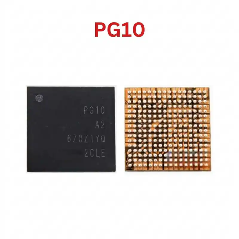
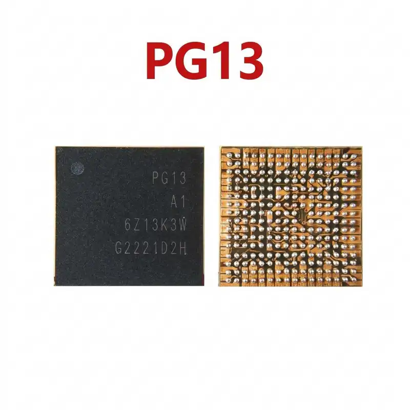
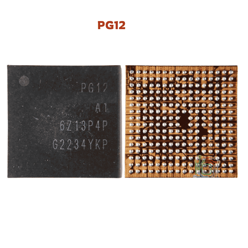
PG11 IC
As low as
Rs 600.00
Worldwide shipping · Cash on Delivery
Product Details
====================================================================================================
PG11 SECONDARY POWER MANAGEMENT & VOLTAGE REGULATOR IC GUIDE
====================================================================================================
1. PRODUCT IDENTIFICATION & HARDWARE SPECIFICATIONS:
----------------------------------------------------------------------------------------------------
- Part Number: PG11 (Top laser silkscreen marking: "PG11")
- IC Product Family: PG-Series Mobile Power & Auxiliary Voltage Regulators
- Silicon Manufacturer: SGMICRO / Mobile Power Management Technology Partners
- IC Classification: Auxiliary PMIC & Low-Noise Subsystem LDO Regulator
- Package Type: WLCSP / Miniature Micro-BGA (Wafer-Level Chip Scale Package)
- Solder Ball Layout: Ultra-Compact Micro-BGA Grid
- Input Voltage Range (VIN): 3.3V – 4.35V DC (Connected directly to system VPH_PWR / VBAT rail)
- Regulated Output Rails: Dual Clean LDO Outputs: 1.8V (VIO Digital Logic) & 2.8V / 3.0V (Analog)
- Output Current Capacity: Up to 300mA – 500mA per regulated channel
- Stencil Compatibility: Amaoe Universal 0.12mm Mobile PMIC / Secondary Power Stencil
- Recommended Solder Paste: 183°C Leaded Solder Paste (Sn63/Pb37)
- Hot Air Rework Settings: 300°C – 320°C (Airflow: 35% – 45%)
2. CIRCUIT ARCHITECTURE & MOTHERBOARD ROLE:
----------------------------------------------------------------------------------------------------
- Touchscreen & Sensor Power Supply: Steps down noisy VPH_PWR battery voltage into ultra-clean,
ripple-free 1.8V and 2.8V rails for touch digitizer controllers and biometric sensor ICs.
- Analog Noise Isolation: Blocks high-frequency RF switching transients generated by modem/PA circuits
from leaking into sensitive image sensors and audio sub-circuits.
- Power Sequencing: Wakes up via enable control lines (EN) routed from the master PMIC or CPU GPIO
lines when the screen panel active state is asserted.
- Target Smartphone Platforms:
* Modern 4G and 5G Android smartphones (Oppo Reno/A series, Vivo V/Y series, Xiaomi Redmi,
Realme, and Transsion/Infinix boards).
3. COMMON MOTHERBOARD FAULT SYMPTOMS:
----------------------------------------------------------------------------------------------------
- Touchscreen Failure / Ghost Touch: Display graphics appear normally, but touch input is completely
unresponsive or suffers erratic phantom touches due to missing/noisy 2.8V VDD_TOUCH from PG11.
- Camera Initialization Failure: Opening the camera triggers instant app crashes or "Camera Hardware
Busy" error due to missing sensor analog voltage.
- Standby Current Leakage (0.05A – 0.12A): Damaged pass-FET inside PG11 drains battery continuously
while the device is locked/sleeping, generating localized warmth around the IC.
- Dead Handset / VPH Short: Severe electrical overstress punctures the internal VIN-to-GND circuit,
collapsing the primary system power rail to 0V.
4. STEP-BY-STEP DIAGNOSTIC & TESTING PROCEDURES:
----------------------------------------------------------------------------------------------------
A. Cold Testing (Multimeter Diode Mode):
1. Disconnect battery and charging cable completely.
2. Set digital multimeter to Diode Mode.
3. Place RED probe on motherboard ground shield (GND) and probe test points around PG11:
- VIN Input Decoupling Capacitor: Normal reading is 380mV – 480mV.
- 1.8V Digital Rail Capacitor: Normal reading is 420mV – 540mV.
- 2.8V / 3.0V Sensor Rail Capacitor: Normal reading is 480mV – 620mV.
4. Diagnostic Rule: If any rail beeps with 000mV – 010mV, isolate whether the filter capacitor
or PG11 itself is shorted by applying rosin and injecting rated voltage.
B. Hot Testing (Live Operating Voltage Check):
1. Connect device to DC power supply set at 4.0V.
2. Verify that 4.0V VPH_PWR is present at the PG11 input capacitor.
3. Press Power Key and unlock screen:
- Check 1.8V line: Must remain solid without dipping.
- Check 2.8V line: Must rise immediately upon display activation.
4. Diagnostic Rule: If VIN is 4.0V, enable line is 1.8V, but outputs read 0V, PG11 is burned out
and must be replaced.
5. REWORK, REBALLING & INSTALLATION GUIDELINES:
----------------------------------------------------------------------------------------------------
- Thermal Protection & Masking:
* Shield surrounding sensitive ICs (CPU, eMMC/UFS, camera connectors) with polyimide tape.
- Chip Removal:
* Apply high-grade tacky BGA flux around the chip edges.
* Use a hot air rework station at 305°C – 315°C with 40% airflow.
* Apply gentle, uniform heat in circular motions. Lift vertically with fine tweezers as soon as
all solder balls melt to preserve motherboard copper pads.
- PCB Pad Preparation:
* Clean pads flat using a soldering iron (300°C) with copper solder wick.
* Clean flux residue thoroughly with 99% Isopropyl Alcohol (IPA).
- Reballing & Installation:
* Reball replacement IC using a 0.12mm universal stencil and 183°C solder paste.
* Apply a microscope-thin film of flux to motherboard pads.
* Position PG11 carefully matching Pin 1 index dot with the silkscreen indicator.
* Heat gently at 300°C until the solder balls fuse and surface tension snaps the IC into alignment.
====================================================================================================
You may also like