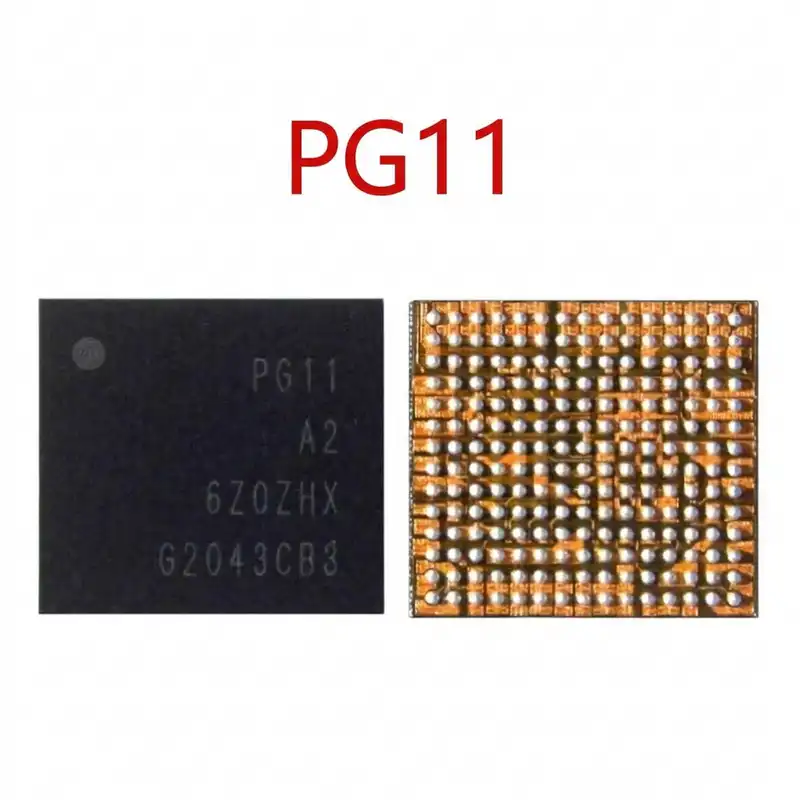
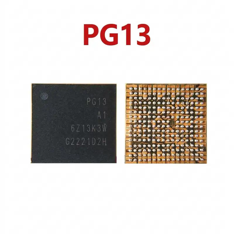
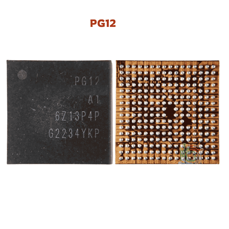
PG10 IC
As low as
Rs 500.00
Worldwide shipping · Cash on Delivery
Product Details
====================================================================================================
PG10 SECONDARY POWER MANAGEMENT & VOLTAGE REGULATOR IC GUIDE
====================================================================================================
1. PRODUCT IDENTIFICATION & HARDWARE SPECIFICATIONS:
----------------------------------------------------------------------------------------------------
- Part Number: PG10 (Silkscreen laser marking on package: "PG10")
- IC Product Family: PG-Series Mobile Power & Auxiliary Voltage Regulators (PG10 - PG15)
- Silicon Manufacturer: SGMICRO / Mobile Power Management Technology Partners
- IC Classification: Subsystem Auxiliary PMIC & Multi-Rail LDO Voltage Regulator
- Package Type: WLCSP / Miniature Micro-BGA (Wafer-Level Chip Scale Package)
- Solder Ball Grid: High-Density Micro-BGA Array
- Input Supply Voltage (VIN): 3.3V – 4.35V DC (Sourced from main system VPH_PWR / VBAT rail)
- Regulated Output Rails: 1.2V (Logic Core), 1.8V (VIO Digital Bus), 2.8V / 3.0V (Analog/Sensor)
- Reballing Stencil: Amaoe Universal 0.12mm Mobile PMIC / Secondary Power Stencil
- Recommended Solder Paste: 183°C Leaded Solder Paste (Sn63/Pb37)
- Hot Air Rework Settings: 300°C – 320°C (Airflow: 35% – 45%)
2. CIRCUIT ARCHITECTURE & MOTHERBOARD ROLE:
----------------------------------------------------------------------------------------------------
- Auxiliary Subsystem Powering: Dedicated to supplying stable, noise-free DC rails to secondary
peripheral logic circuits, such as camera image signal processors (ISP), biometric sensors, and
audio/RF interface circuits.
- Power Sequencing Handshake: Operates under control of the primary PMIC (Qualcomm PM or MediaTek MT);
activates secondary voltage rails sequentially only after the base CPU kernel wakes up.
- Power Good (PGOOD) Acknowledgment: Returns a high-logic acknowledgment signal to the main processor
confirming peripheral power stability.
- Compatible Smartphone Handsets:
* Widely deployed on modern 4G and 5G Android motherboards including Oppo, Vivo, Xiaomi/Redmi,
Realme, and Transsion (Infinix, Tecno) mid-range platforms.
3. COMMON MOTHERBOARD FAULT SYMPTOMS:
----------------------------------------------------------------------------------------------------
- Handset Boot Loop / Hanging on Logo: Device attempts to boot, displays the brand logo, but resets
repeatedly because the main CPU fails to receive the PGOOD voltage confirmation from PG10.
- Peripheral Function Failure: Camera application crashes with "Unable to connect to camera", or the
in-display / side fingerprint sensor is completely unrecognized in device settings.
- Secondary Battery Drain (0.05A – 0.15A Leakage): An internal short or leakage across PG10 output
channels pulls continuous current from the battery in sleep mode, keeping the board warm.
- Total Dead Handset (VPH Rail Punctured): A severe short between VIN and GND inside the IC drops the
entire primary system voltage to 0V, preventing the phone from drawing boot current.
4. STEP-BY-STEP DIAGNOSTIC & TESTING PROCEDURES:
----------------------------------------------------------------------------------------------------
A. Cold Testing (Multimeter Diode Mode):
1. Disconnect battery and charger.
2. Set digital multimeter to Diode Mode.
3. Place RED probe on motherboard ground shield (GND) and probe filtering capacitors around PG10:
- VIN Input Line: Normal reading is 380mV – 480mV.
- 1.8V VIO Line: Normal reading is 420mV – 550mV.
- 2.8V / 3.0V Auxiliary Rails: Normal reading is 500mV – 650mV.
4. Fault Evaluation: If any capacitor gives a continuous beep (000mV – 010mV), identify whether
the capacitor or PG10 is shorted by injecting low voltage (1.0V–1.8V) and checking with rosin.
B. Hot Testing (Live Operating Voltage Check):
1. Connect handset to DC Power Supply set at 4.0V.
2. Verify that 4.0V VPH_PWR is present at the PG10 input decoupling capacitor.
3. Press the Power Key: Monitor oscilloscope or multimeter on output coils/capacitors.
4. Diagnostic Rule: PG10 must generate stable 1.8V and 2.8V rails during the boot stage. If input
voltage and enable signals are present but outputs remain at 0V, replace PG10.
5. REWORK, REBALLING & INSTALLATION GUIDELINES:
----------------------------------------------------------------------------------------------------
- Thermal Masking & Precaution:
* Apply polyimide thermal tape over nearby memory chips (eMMC / UFS), cameras, and CPU to prevent
collateral desoldering.
- Chip Removal:
* Apply a small amount of high-grade tacky BGA flux around the chip boundary.
* Use a hot air rework station at 305°C – 315°C with moderate 40% airflow.
* Heat evenly in circular motions. Lift vertically with fine tweezers as soon as all solder balls melt.
- PCB Pad Preparation:
* Use a soldering iron at 300°C with copper solder wick to clean the motherboard pads flat.
* Wash with Isopropyl Alcohol (IPA) and inspect under microscope for broken or bridged pads.
- Reballing & Installation:
* Reball the replacement IC using a 0.12mm universal stencil and 183°C leaded solder paste.
* Apply a thin film of flux on PCB pads. Align Pin 1 index dot precisely according to board silkscreen.
* Apply gentle heat at 300°C until the solder balls melt and surface tension pulls PG10 into exact
self-alignment. Allow the board to cool before powering on.
====================================================================================================
You may also like