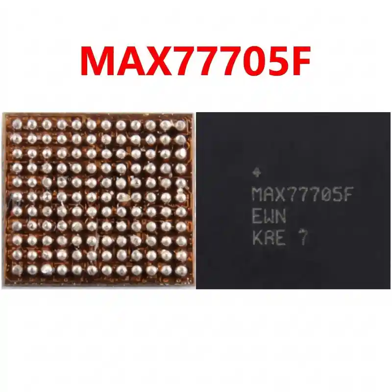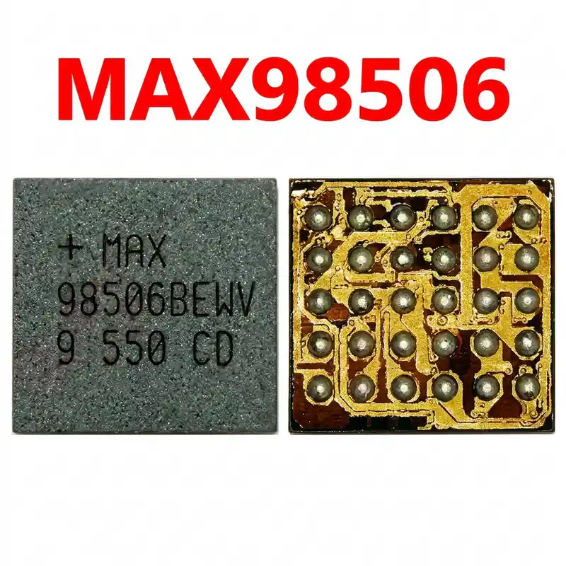

MAX77910-11 IC
As low as
Rs 0.00
Worldwide shipping · Cash on Delivery
Product Details
1. ARCHITECTURAL OVERVIEW
The SKY77910-11 is a fully integrated RF Front-End Module (FEM) combining GaAs Heterojunction Bipolar Transistor (HBT) power amplifier blocks, a silicon CMOS controller, and a high-linearity, low-loss pseudomorphic High Electron Mobility Transistor (pHEMT) antenna switch matrix. It features integrated directional coupling (eliminating external couplers), 0V DC offset TRx ports (eliminating DC blocking capacitors), and internal 50-ohm impedance matching networks on all RF input and output paths.
2. HARDWARE DIAGNOSTICS & FAULT ISOLATION
A. Cold Checks (Multimeter in Diode Mode, Red probe on Ground, Black probe on test point):
- Measure decoupling capacitors adjacent to the IC connected to the main battery rail (VBAT):
* Normal drop: ~0.350V - 0.450V.
* Short circuit (< 0.050V): Indicates internal punch-through of GaAs PA stages to ground.
- Measure MIPI control lines (SCLK, SDATA) and VIO (1.8V):
* Normal drop: ~0.400V - 0.600V.
* Open circuit (OL) or short to ground indicates broken solder pads or defective bus pull-ups.
B. Hot Checks (DC Power Supply connected with current limit set to 2.0A):
- Monitor standby current: A leaking internal PA stage typically draws 50mA to 250mA immediately before power button trigger.
- During GSM 900/1800 transmission or outgoing emergency call attempt, probe VRAMP and VBAT rails. If current spikes abnormally (>1.5A) followed by device reset, the PA is internally degraded.
3. SAFETY & THERMAL PROTECTION PROTOCOLS
- The SKY77910-11 is constructed as a multi-layer laminate substrate with plastic overmolding. Excessive localized heat will cause blistering or pad separation.
- Adjacent Components: RF baseband transceivers (MT61xx series) and sensitive crystal oscillators (26 MHz / 38.4 MHz TCXO) are typically positioned within 5mm to 10mm. Shield adjacent silicon, RAM/EMMC, and plastic SIM/tray connectors with multi-layer Kapton tape topped with aluminum heat-sink foil.
4. STEP-BY-STEP REWORK PROCEDURE
A. IC Removal:
- Apply a light, uniform coat of high-grade tacky no-clean rosin flux (e.g., NC-559).
- Hot Air Settings: 320°C - 340°C (depending on station efficiency and nozzle diameter: 6mm - 8mm recommended) with 40-50% airflow.
- Pre-heat the entire PCB section evenly around the RF shield area from 150°C to 180°C for 20-30 seconds to prevent board warpage.
- Direct air vertically at the perimeter of the IC in continuous small circular motions.
- Test melt status using fine tweezers on an adjacent passive component. Once solder reaches liquidus (around 217°C for lead-free SAC305), gently lift the IC straight upward. Never twist or pry cold pads.
B. PCB Pad Preparation:
- Apply fresh flux to the PCB footprint.
- Use a calibrated soldering iron with a bevel/knife tip at 330°C and fine copper desoldering braid.
- Level the central ground pad array and perimeter signal pads without applying downward pressure to avoid peeling delicate laminate copper traces.
- Clean the area using 99.9% anhydrous Isopropyl Alcohol (IPA) and inspect under microscope for bridged vias or lifted solder mask.
C. Reballing / Stenciling:
- Use a dedicated 77910 stencil or a universal 0.35mm/0.40mm LGA/BGA stencil.
- Recommended paste: Low-to-medium melt leaded paste (Sn63/Pb37, melting point 183°C) for maximum reliability during field repair, or standard lead-free SAC305 (217°C).
- Scrape paste across stencil apertures, wipe clean, and heat uniformly at 260°C - 280°C with low airflow (15-20%) until balls form.
- Clean flux residue and inspect bump height uniformity under microscope.
D. Installation & Alignment:
- Coat the motherboard footprint with an ultra-thin film of tacky flux (excess flux will cause the lightweight LGA IC to float or shift out of alignment).
- Align Pin 1 orientation index (chamfered corner / laser dot) to the PCB silkscreen orientation marking.
- Heat vertically at 320°C - 330°C with moderate airflow (30%).
- Observe solder reflow: The surface tension will visibly pull the IC into center alignment ("self-centering"). Give an extremely light side-nudge with tweezers; the chip must spring back instantly into place.
- Remove heat immediately and allow natural cooling for at least 90 seconds without moving the board.
5. POST-INSTALLATION VALIDATION
- Perform cold diode mode measurements on the VBAT input capacitors to ensure zero solder bridges to ground.
- Clean residual flux using a soft ESD brush and IPA.
- Reassemble antenna coaxial cables, verify RF ground clip continuity to the phone chassis, power up the handset, and test 2G/3G/4G registration, incoming/outgoing call voice stability, and data throughput.
You may also like