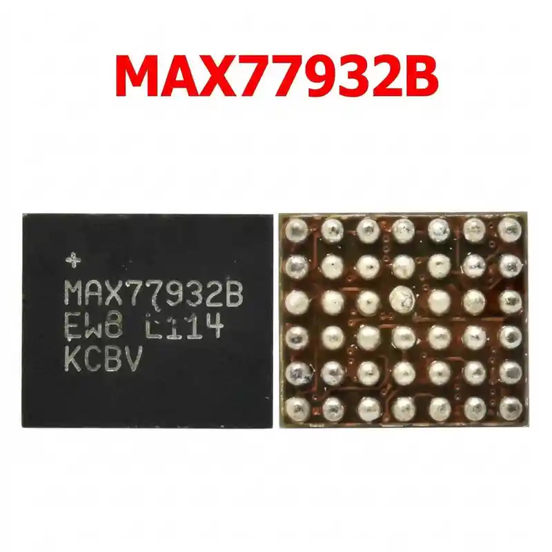
MAX98506BEWV IC
As low as
Rs 0.00
Worldwide shipping · Cash on Delivery
Product Details
--------------------------------------------------------------------------------
SECTION 1: INTERNAL ARCHITECTURE & SIGNAL TOPOLOGY
--------------------------------------------------------------------------------
1. Functional Blocks:
- High-Efficiency Class-D Output Stage: Direct differential bridge-tied load (BTL) drive lines (OUTP / OUTN) connected to the bottom loudspeaker springs.
- Integrated Synchronous DC-DC Boost Converter: Automatically boosts input battery voltage (VBAT 3.0V - 4.35V) up to an elevated internal rail (~8.5V - 10V DC) during high-amplitude audio peaks to prevent distortion and clipping.
- Digital Audio / Control Interface: Receives digital audio over I2S / PDM bus from the application processor (Exynos 8895 / Snapdragon 835) and volume/configuration commands via I2C control bus (SDA / SCL).
- Built-in Protection Engine: Over-current protection (OCP), over-temperature thermal shutdown, and speaker impedance monitoring.
--------------------------------------------------------------------------------
SECTION 2: STEP-BY-STEP MULTIMETER TESTING & DIAGNOSTICS
--------------------------------------------------------------------------------
1. Cold Resistance Testing (Diode Mode Readings - RED probe to GND, BLACK probe on test points):
- Loudspeaker Output Pads (SPK+ / SPK- test points near the bottom speaker contacts):
* Normal Reading: ~450 mV to 550 mV on both lines (Both lines must show balanced values within ±10 mV).
* Short Circuit Fault: 0.000V indicates punctured BTL output MOSFET inside MAX98506.
* Open Circuit (OL): Indicates burned series ferrite filter beads between IC and speaker contacts.
- VBAT Main Supply Capacitors (Adjacent to MAX98506):
* Normal Reading: ~380 mV to 490 mV (Reverse mode must read OL / Infinite).
* Short Circuit Fault: 0.000V confirms shorted internal boost converter section; phone will be completely dead.
- Boost Flying / Output Capacitor:
* Normal Reading: ~450 mV to 600 mV.
- I2C Control Bus (SDA / SCL):
* Normal Reading: ~420 mV to 540 mV on both lines.
2. Hot Voltage Testing (Board Powered ON with Ringtone / Media Playing):
- Measure VBAT supply capacitor: Must read steady battery voltage (+3.8V to +4.3V DC).
- Measure Boost Output Capacitor during high-volume media playback: Voltage should dynamically boost up to +7.5V - +9.5V DC. If voltage remains flat at 3.8V, the internal boost generator of MAX98506 is dead.
--------------------------------------------------------------------------------
SECTION 3: DESOLDERING, REBALLING & REWORK SPECIFICATIONS
--------------------------------------------------------------------------------
1. Safe Removal:
- Samsung Galaxy S8/S8+ motherboards have Exynos/Snapdragon CPU and UFS memory nearby. Always apply heat-reflective Kapton tape and thick aluminum foil over the CPU and neighboring connectors.
- Apply a drop of quality tacky flux (Amtech NC-559 or Relife RL-422) around MAX98506.
- Hot Air Settings: Set temperature to 330°C - 340°C with 20% - 25% airflow.
- Heat in a smooth, continuous circular motion for 10–12 seconds until all 30 BGA micro-balls liquefy; lift vertically with fine-tip tweezers.
2. PCB Pad Preparation:
- Apply 183°C leaded solder wire (Sn63/Pb37) to the 30 motherboard pads at 300°C using a micro-soldering tip to soften lead-free factory solder.
- Gently sweep flat with 0.6mm desoldering braid without applying downward pressure.
- Clean the area thoroughly with 99.9% pure Isopropyl Alcohol (IPA) and verify under microscope that all pads are clean, intact, and separated.
3. Reballing & Installation of New MAX98506:
- Use a dedicated Samsung S7 / S8 audio BGA stencil (Amaoe SAM series, 0.12mm thickness).
- Apply 183°C solder paste smoothly; heat with hot air at 250°C to form uniform spherical micro-balls.
- Apply a micro-thin layer of tacky flux on the cleaned motherboard pads.
- Align Pin 1 corner index dot precisely with the white silkscreen dot on the motherboard.
- Solder with hot air at 310°C - 320°C with low airflow (15% - 20%) until surface tension centers the chip onto the footprint.
- Allow natural cooling for 2 minutes, clean flux residue with IPA, assemble the board, connect the speaker, and verify loud, clear media and ringer audio at full volume.
You may also like