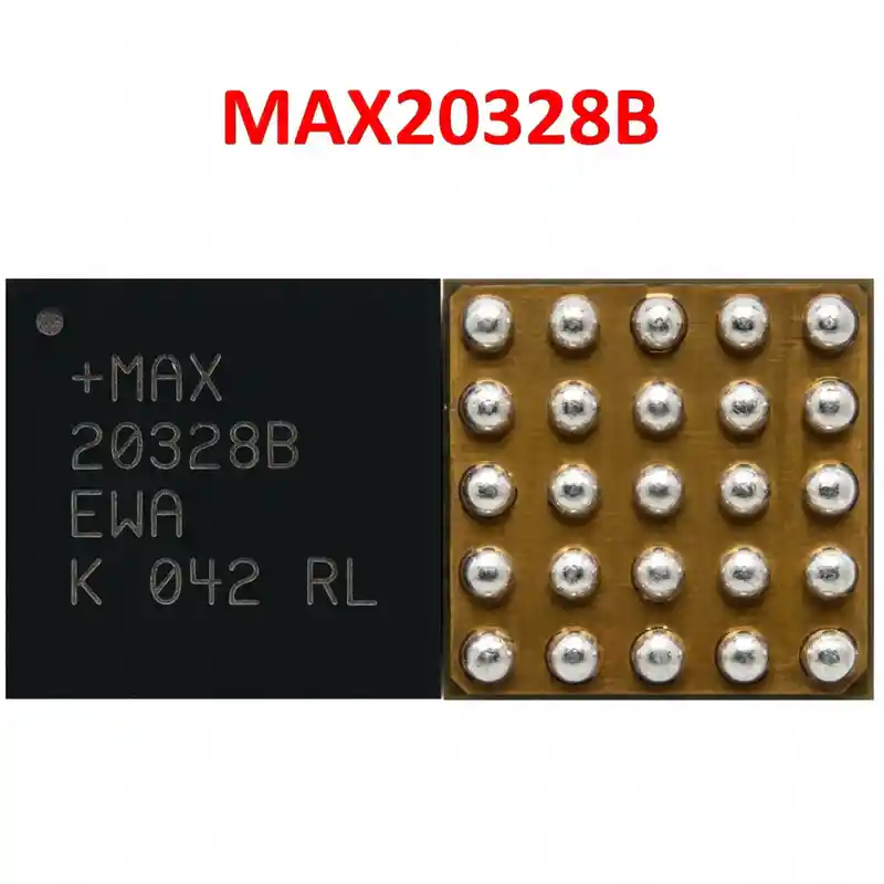
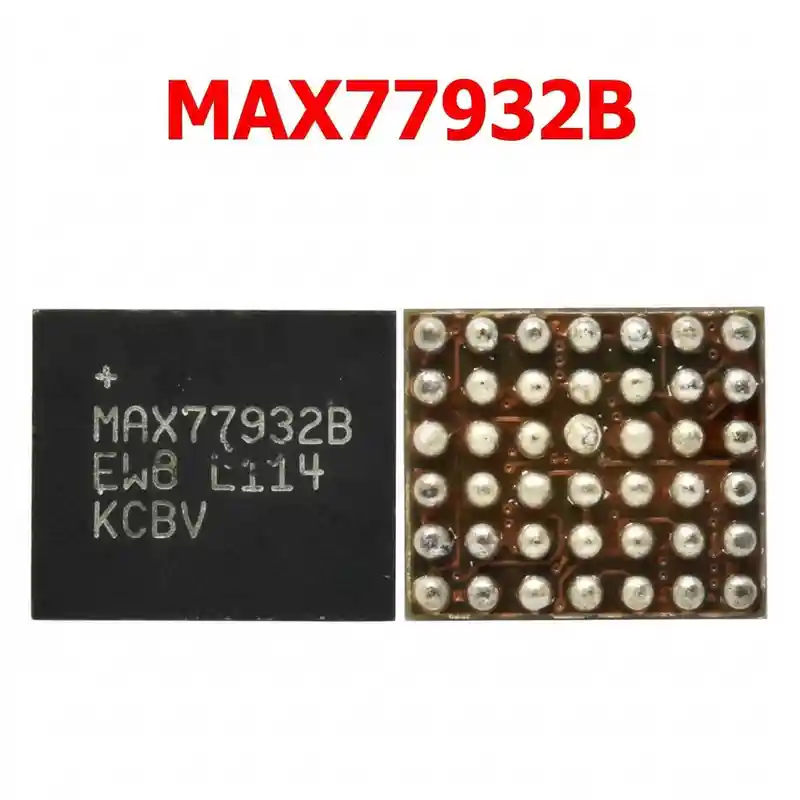
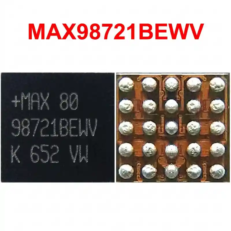
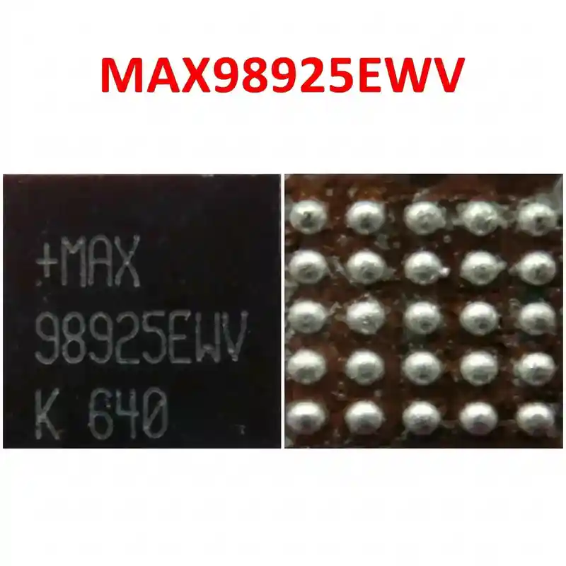
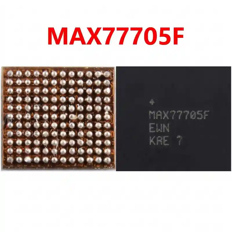
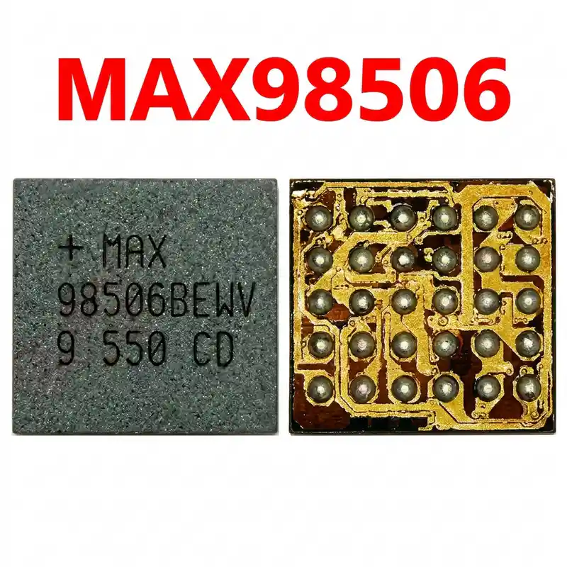
MAX77775 IC
As low as
Rs 0.00
Worldwide shipping · Cash on Delivery
Product Details
1. ARCHITECTURAL & CIRCUIT OVERVIEW
The MAX77775 is an advanced USB Type-C and Power Delivery (PD) interface PMIC deployed in Samsung flagship devices (Galaxy S24/S25 series, Z Flip5/Fold5). Sitting directly behind the USB Type-C connector, it is the first active silicon component to interact with any inserted cable or dock. It manages the CC1/CC2 lines, negotiates Power Delivery profiles (including PPS up to 45W), controls internal high-voltage protection FETs, and communicates status back to the main Application Processor (Exynos 2400 / Snapdragon 8 Gen 3) and secondary charging buck stages via a high-speed I2C/SPMI bus.
2. CHIP-LEVEL HARDWARE DIAGNOSTICS
A. Inline USB Power Meter Diagnostics:
- 0.00A Inactive Draw: Check CC1 and CC2 line values. If the CC pull-down resistors or internal TCPCI logic fail to detect cable attachment, the MAX77775 will not close the internal VBUS power switch.
- 5.0V / 0.45A Fixed Draw: Basic 5V legacy power is passing, but digital PD communication over the CC line is dead. Indicates damaged internal CC transceivers or blown line ESD suppressors.
- Cyclic 0mA -> 400mA -> 0mA Tripping: Internal over-current or short circuit on the downstream power path; the IC enters hiccup protection mode.
B. Cold Diode Mode Testing (Multimeter in Diode Mode, Red probe on Ground, Black probe on test point):
- Measure VBUS input filtering capacitors adjacent to the MAX77775:
* Normal forward voltage drop: ~0.500V - 0.650V.
* Short circuit (< 0.050V): Confirms internal puncture of the input protection FETs to ground.
- Measure CC1 and CC2 test pads / inline chokes:
* Normal forward voltage drop: ~0.550V - 0.700V (must match within 5% symmetry).
* Reading of 0.00V indicates an ESD clamp diode short; OL indicates open circuit between the port and the IC.
- Measure I2C/SPMI lines (SCL, SDA) and 1.8V IO rail:
* Normal forward voltage drop: ~0.420V - 0.550V.
3. THERMAL MANAGEMENT & SPECIAL WLP SAFEGUARDS
- Package Structure: The MAX77775 is a Wafer-Level Chip-Scale Package (WLP) composed of an unencapsulated, ultra-thin bare silicon die with fine-pitch micro-solder balls (0.35mm - 0.40mm pitch).
- Die Fragility: Bare silicon dies crack easily under mechanical strain. Never lever, twist, or apply pinpoint pressure with tweezers on the corners or edges of the die.
- Board Underfill: Samsung flagships use tough, dense epoxy underfill surrounding and anchoring the IC to the multi-layer motherboard. All perimeter underfill must be carefully cleared at 180°C - 200°C prior to chip desoldering.
- Surrounding Protection: On Galaxy S24 series boards, the main AP/DRAM PoP stack, UFS 4.0 storage, secondary PMICs (S2MPS series), and delicate camera FPC connectors reside in close proximity. Mask surrounding areas with double-layer Kapton tape topped with heavy aluminum heat shields.
4. STEP-BY-STEP REWORK PROTOCOL
A. Underfill Removal:
- Secure the motherboard firmly in a precision PCB repair fixture.
- Set hot air rework station to 180°C - 200°C with 30% airflow.
- Heat the periphery of the MAX77775. Using an ultra-fine curved dental hook or dedicated underfill scraper, gently shave away the perimeter black glue without scratching motherboard solder mask or disturbing 0201/01005 surface-mount capacitors.
B. Chip Removal:
- Apply a small amount of premium tacky no-clean BGA flux (e.g., Amtech NC-559-V2 or Kingbo RMA-218).
- Hot Air Settings: 330°C - 350°C with 35-40% airflow (6mm nozzle).
- Pre-heat the entire local PCB section from 4cm distance for 25-30 seconds to reach ~150°C.
- Direct air perpendicularly over the MAX77775 die in steady, small circular motions.
- Once the solder balls liquefy, lift the IC straight upward using precision curved tweezers or a vacuum suction pen. Never slide, pry, or scrape across pads.
C. Motherboard Pad Dressing:
- Apply fresh flux to the PCB footprint.
- Set micro-soldering iron to 310°C - 320°C using a micro-knife (K) or bevel (BC) tip.
- Lightly glide leaded solder wire (Sn63/Pb37) across the pads to dilute the factory high-melt lead-free alloy.
- Use fine copper desoldering braid to gently wick remaining solder flat without applying downward pressure.
- Clean thoroughly with 99.9% anhydrous Isopropyl Alcohol (IPA) and inspect under microscope: verify that all micro-pads are completely flat and solder resist webs between adjacent pads remain 100% intact.
D. Reballing / Stenciling:
- Use a dedicated Samsung S24 PMIC stencil or a universal 0.35mm - 0.40mm WLP BGA stencil.
- Solder Alloy: Medium-melt leaded solder paste (Sn63/Pb37, melting point 183°C).
- Clamp the clean die flat against the stencil, apply paste evenly across all apertures with a scraper, wipe off excess, and reflow with hot air at 250°C - 260°C under low airflow (15%).
- Allow natural cooling, release the stencil, add a micro-drop of flux, and reheat briefly to form perfectly spherical, uniform solder balls.
E. Resoldering & Alignment:
- Apply an ultra-thin, transparent layer of tacky flux across the PCB footprint (excess flux will float the miniature WLP die).
- Align Pin 1 corner index dot precisely with the motherboard silkscreen orientation mark.
- Apply hot air vertically at 320°C - 330°C with 25-30% airflow.
- Watch for solder reflow: The surface tension of molten solder will self-center the chip into exact alignment.
- Give an extremely gentle micro-nudge with the tip of tweezers to confirm spring-back elasticity.
- Remove heat and allow the board to cool down naturally for at least 2 minutes.
5. POST-REWORK VERIFICATION
- Measure diode mode values on VBUS, VSYS, and CC1/CC2 lines to confirm zero shorts or bridges to ground.
- Clean residual flux using an ESD brush and IPA.
- Connect the battery, plug in an official Samsung 25W/45W USB-PD fast charger through an inline power meter.
- Verify automatic USB-PD PPS negotiation (voltage stepping from 5V up to 9V/15V).
- Confirm charging current climbs above 2.0A+, check that the screen displays "Super Fast Charging", and test USB-C data transfer (MTP) and OTG functionality to ensure complete circuit restoration.
You may also like