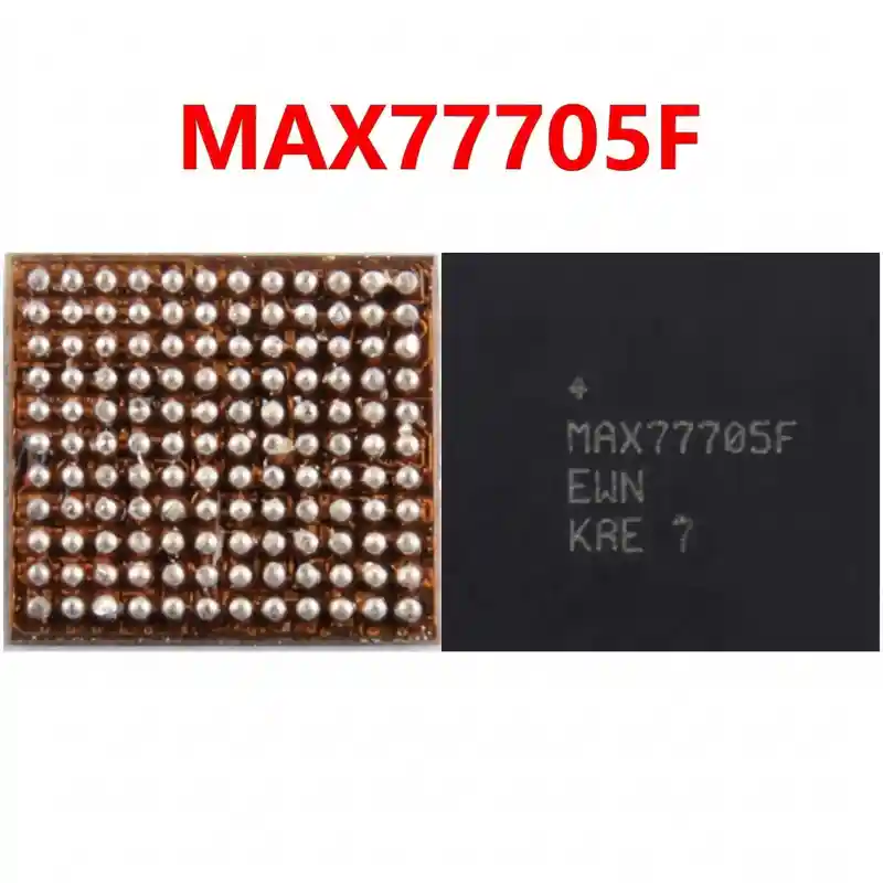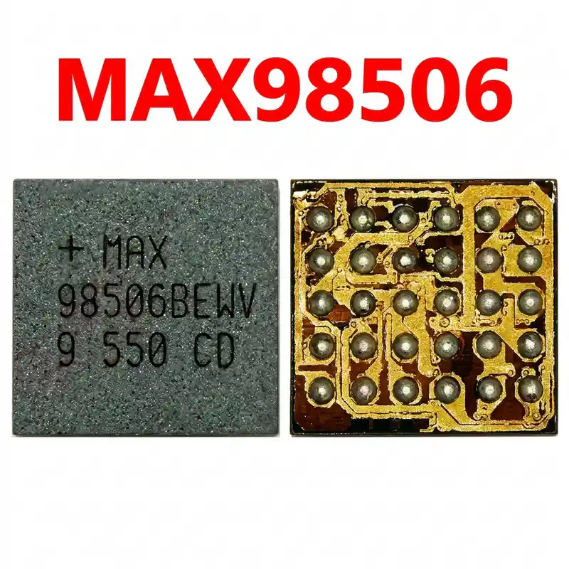

MAX77656-11 IC
As low as
Rs 0.00
Worldwide shipping · Cash on Delivery
Product Details
1. ARCHITECTURAL & CIRCUIT OVERVIEW
The SKY77656-11 is a hybrid Multimode Multiband Power Amplifier Module (MMMB PAM). It houses InGaP/GaAs Heterojunction Bipolar Transistor (HBT) power cores and a silicon CMOS control block on a multi-layer laminate substrate with plastic overmolding. The internal design segregates the 2.5G linear GMSK/EDGE circuitry from the 3G/4G wideband paths to optimize Power-Added Efficiency (PAE). All RF ports feature integrated DC-blocking capacitors and 50-ohm internal matching. It receives supply power directly from the main battery rail (VBAT/VPA) managed by an external APT DC-DC converter, along with 1.8V VIO for the digital MIPI RFFE control bus.
2. HARDWARE DIAGNOSTICS & FAULT ISOLATION
A. Cold Diode Mode Testing (Multimeter in Diode Mode, Red probe on Ground, Black probe on test point):
- Locate large filter bypass capacitors adjacent to the SKY77656-11 on the VBAT/VPA power input line:
* Normal forward voltage drop: ~0.350V - 0.460V.
* Direct short (< 0.050V): Confirms internal punch-through of the GaAs PA output stage to the substrate ground.
- Probe the MIPI RFFE clock and data lines (RFFE_CLK, RFFE_DATA) and the 1.8V VIO rail:
* Normal forward voltage drop: ~0.400V - 0.550V.
* Open circuit (OL) indicates fractured LGA solder pads or severed motherboard traces; 0.00V indicates a shorted digital controller.
B. Hot Testing (Connected to Regulated DC Bench Power Supply set to 4.0V, 2.5A limit):
- Standby Current: Observe current before pressing the power button. An undamaged board draws 0.000A. A degraded or leaking 77656-11 typically draws between 70mA and 350mA without power trigger.
- Active Call Testing: Power on the device and initiate a voice or emergency call (*#112 / *#911). If current spikes abruptly above 1.8A followed by immediate shutdown, battery disconnect, or system freeze, the PA is internally shorting under transmit envelope modulation.
3. THERMAL MANAGEMENT & SURROUNDING PROTECTION
- The SKY77656-11 is housed in a 4.30mm x 6.95mm multi-layer organic laminate substrate encapsulated in plastic resin. Due to its rectangular geometry, uneven heating will cause warping, corner lifting, or internal substrate delamination.
- Critical Adjacent Components: On Samsung Note 8, S9, and A50 motherboards, the Shannon RF transceiver, 26 MHz TCXO crystal oscillator, intermediate SAW duplexers, power management ICs, and plastic SIM card trays are situated within 4mm to 10mm of the PA.
- Thermal Masking: Apply two layers of polyimide (Kapton) tape over adjacent components, covered with a layer of aluminum foil or a copper heat-sink coin to shield surrounding silicon and prevent thermal drift in the reference clock.
4. STEP-BY-STEP REWORK PROTOCOL
A. Desoldering / Removal:
- Apply a small amount of high-grade tacky no-clean BGA flux (e.g., Amtech NC-559-V2 or Kingbo RMA-218) along the periphery of the rectangular IC.
- Hot Air Rework Station Settings: 330°C - 350°C (depending on station thermal transfer efficiency, 6mm - 8mm nozzle) with 40-50% airflow.
- Pre-heat the entire RF zone from a distance of 4cm - 5cm for 25-30 seconds to bring local PCB temperature to ~150°C and minimize thermal shock.
- Move the hot air nozzle in an elongated oval pattern covering the full 6.95mm length of the SKY77656-11 uniformly.
- Test solder melt status on adjacent passive capacitors with curved micro-tweezers. Once solder reaches liquidus (around 217°C for factory lead-free alloy), gently lift the IC straight upward. Never slide, tilt, or pry cold pads.
B. Motherboard Pad Dressing:
- Apply fresh flux to the 40-pad PCB footprint.
- Using a knife or hoof soldering iron tip set at 320°C and clean copper desoldering wick, gently absorb residual lead-free solder. Keep the tip flat to avoid scratching solder mask bridges between the closely spaced 40 LGA pads.
- Clean the area thoroughly with 99.9% anhydrous Isopropyl Alcohol (IPA) and an ESD brush. Inspect under microscope to ensure zero lifted pads, exposed ground copper, or burnt flux residue.
C. Reballing / Stenciling:
- Use a dedicated 77656-11 stencil or a universal 0.35mm - 0.40mm LGA/BGA stencil matching the 4.30mm x 6.95mm 40-pad layout.
- Recommended Solder Alloy: Medium-temperature leaded paste (Sn63/Pb37, melting point 183°C) for maximum mechanical flexibility and resilience against thermal cycling.
- Spread paste evenly across all 40 apertures using a squeegee, wipe off excess paste, hold stencil flat, and reflow at 260°C - 280°C with low airflow (15-20%).
- Allow to cool, release stencil, and verify uniform solder ball height under microscope.
D. Resoldering & Alignment:
- Coat the motherboard footprint with an ultra-thin film of tacky flux (excess flux will cause the elongated LGA package to float or drift).
- Align Pin 1 orientation index (chamfered edge / laser dot marker) precisely with the PCB silkscreen reference mark.
- Apply hot air vertically at 320°C - 330°C with 30-35% airflow, moving along the length of the package.
- Observe solder reflow: The surface tension of molten solder will pull the IC into central alignment ("self-centering").
- Perform a micro-nudge test with tweezers: touch the corner gently; if it springs back instantly into alignment, reflow is complete.
- Remove heat immediately and allow natural cooling for 90 seconds without moving the board.
5. POST-REWORK VERIFICATION
- Measure resistance and diode mode value on the VBAT/VPA decoupling capacitors to confirm zero solder bridges to ground.
- Clean residual flux using an ESD brush with IPA.
- Connect cellular coaxial antenna cables and inspect RF grounding clip contacts to the chassis.
- Insert an active SIM card, power up the handset, and dial *#0011# (Samsung Service Mode) or *#*#4636#*#* to access the Phone Information engineering menu.
- Verify 2G, 3G, and 4G LTE band registration, confirm RSRP / RSSI signal levels, test outgoing/incoming voice calls, and run a cellular data throughput test to confirm sustained RF transmit/receive stability.
You may also like