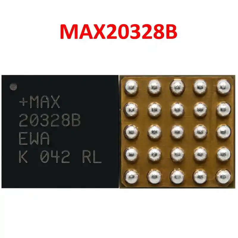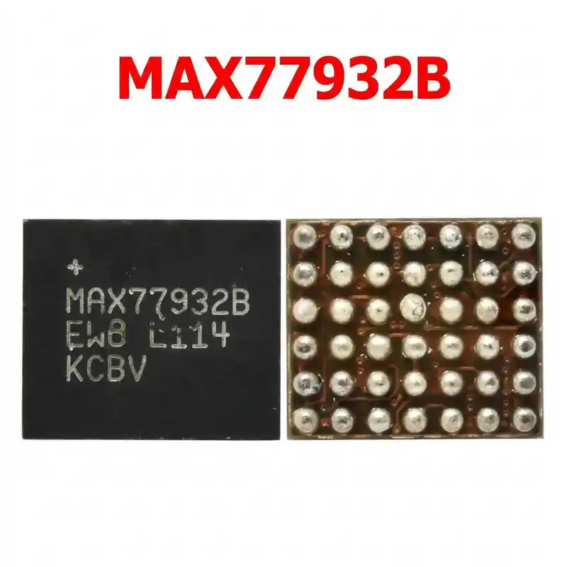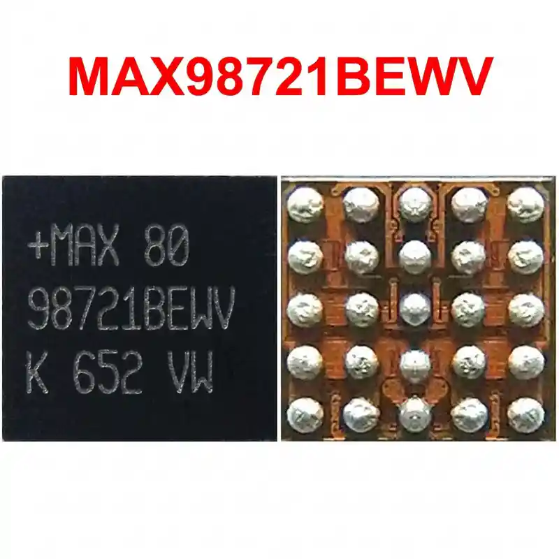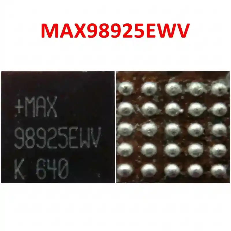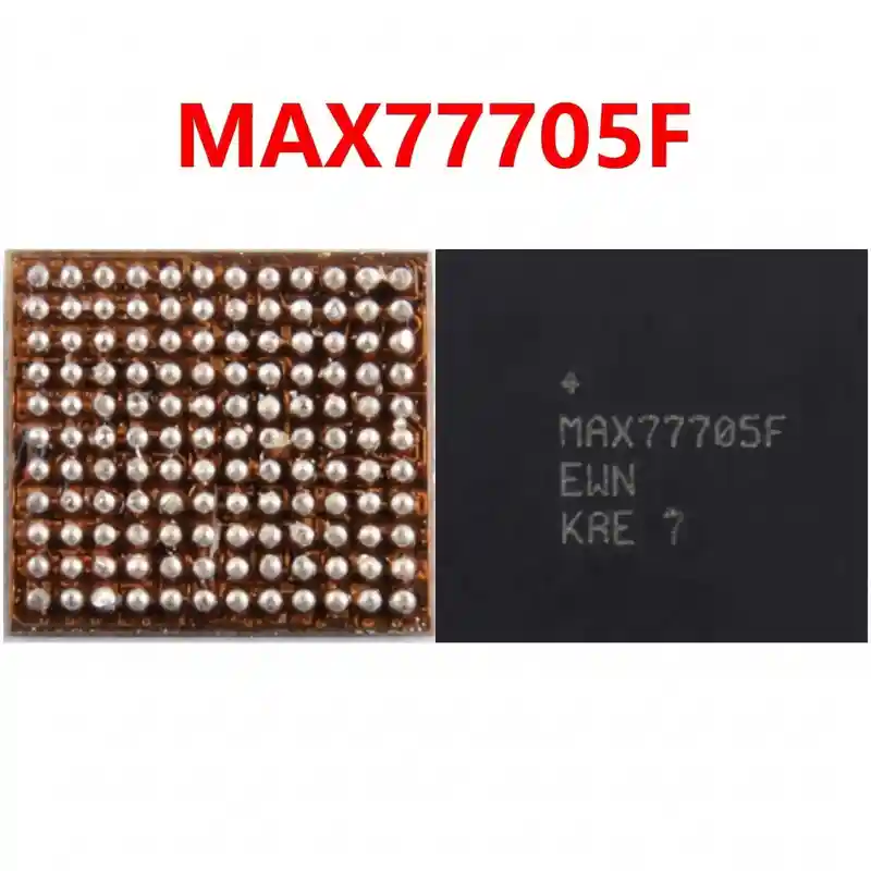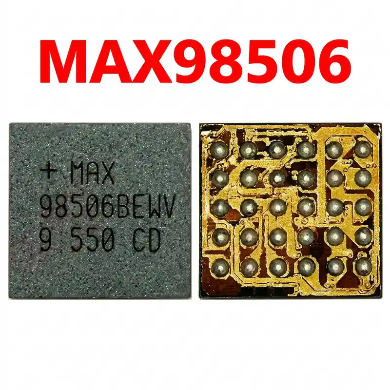

MAX77648-11 IC
As low as
Rs 0.00
Worldwide shipping · Cash on Delivery
Product Details
--------------------------------------------------------------------------------
SECTION 1: INTERNAL ARCHITECTURE & RF POWER TOPOLOGY
--------------------------------------------------------------------------------
1. Functional Blocks:
- Heterojunction Bipolar Transistor (InGaP HBT) Power Cores: High-linearity multi-stage amplification covering Low-Band, Mid-Band, and High-Band cellular transmission.
- Integrated Band-Switching & Duplexer Matrix: Selects active transmission frequency path and directs amplified power to corresponding antenna matching filters.
- MIPI RFFE Serial Control Bus: Dual-line digital interface (VIO 1.8V, SCLK, SDATA) managed by the baseband modem for real-time power level shifting, mode selection, and band control.
- Average Power Tracking (APT) Interface: Integrates with external DC-DC tracking regulator to modulate supply voltage dynamically according to RF output power demand, reducing heat and battery consumption.
--------------------------------------------------------------------------------
SECTION 2: STEP-BY-STEP MULTIMETER TESTING & DIAGNOSTICS
--------------------------------------------------------------------------------
1. Cold Resistance Testing (Diode Mode Readings - RED probe to GND, BLACK probe on test points):
- VPA / VBAT Main Power Input Capacitors (Large filter capacitors beside SKY77648):
* Normal Reading: ~360 mV to 480 mV (Reverse mode must read OL / Infinite).
* Short Circuit Fault: 0.000V indicates punctured HBT power stage; causes full battery line short and dead phone.
- VIO 1.8V Logic Reference Capacitor:
* Normal Reading: ~450 mV to 580 mV.
- MIPI RFFE Control Lines (CLK / DATA):
* Normal Reading: ~480 mV to 600 mV on both lines (Must be balanced within ±20 mV).
- RF Input / Output Filter Lines:
* Normal Reading: ~400 mV to 550 mV on active side; capacitive open circuit on AC-coupled RF lines.
2. Hot Voltage Testing (Board Powered with SIM Card Inserted):
- Measure VPA supply rail: Must read steady +3.4V to +4.0V DC.
- Make an outgoing phone call (or dial 112 emergency call):
* Current should pulse between 180mA and 450mA during cellular bursts.
* Diagnostic Rule: If signal drops from full bars to "No Service" or phone instantly shuts down the moment a call connects, the internal power amplifier stage of SKY77648-11A is blown and must be replaced.
--------------------------------------------------------------------------------
SECTION 3: DESOLDERING, REBALLING & REWORK SPECIFICATIONS
--------------------------------------------------------------------------------
1. Safe Removal:
- RF PA modules feature a large ground thermal pad underneath that dissipates heat rapidly. Shield neighboring CPU, eMMC/UFS, and sensitive crystal oscillators with heat-reflective Kapton tape and thick aluminum shield.
- Apply a drop of quality tacky flux (Amtech NC-559 or Relife RL-422) around SKY77648.
- Hot Air Settings: 330°C - 340°C with 25% airflow.
- Heat in a smooth, continuous circular motion for 15–20 seconds until the center ground pad liquefies completely; lift vertically with fine-tip tweezers.
2. PCB Footprint Preparation:
- Apply 183°C leaded solder wire (Sn63/Pb37) to the motherboard pads at 300°C using a micro-chisel tip to soften lead-free factory solder.
- Gently sweep flat with 0.8mm desoldering braid to make the center ground plane and outer pads completely level.
- Clean the area thoroughly with 99.9% pure Isopropyl Alcohol (IPA) and inspect under microscope for any pad bridging or residual flux.
3. Reballing & Installation of New SKY77648-11A:
- Factory new chips in blister tape come pre-tinned. If re-using a chip, use a universal PA BGA stencil (0.12mm thickness) with 183°C solder paste.
- Apply a micro-thin layer of tacky flux on the cleaned motherboard pads.
- Align Pin 1 corner index dot precisely with the white silkscreen dot on the motherboard.
- Solder with hot air at 315°C - 325°C with low airflow (15% - 20%) until surface tension centers the chip onto the footprint. Give a light side-tap to confirm molten state.
- Allow natural cooling for 2 minutes, clean flux residue with IPA, firmly reconnect all coaxial RF antenna cables, assemble the housing, and test 3G/4G signal stability and outgoing calls.
You may also like