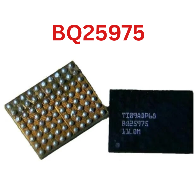
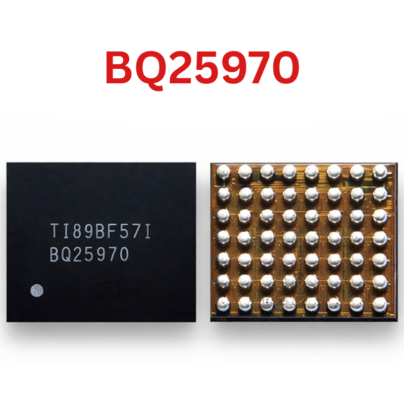
BQ25975 IC
As low as
Rs 0.00
Worldwide shipping · Cash on Delivery
Product Details
1. ARCHITECTURAL OVERVIEW & CIRCUIT BEHAVIOR
The BQ25975 is a single-cell battery charge controller built on Texas Instruments' dual-phase switched-capacitor topology. In modern mobile charging topologies, it operates in parallel with a traditional buck charger PMIC (such as BQ2589x or Qualcomm SMB series):
- Primary Buck Charger Role: Manages battery pre-charging, trickle charging, USB input detection, system rail generation (VSYS), and constant voltage (CV) tapering.
- BQ25975 Switched-Capacitor Role: Takes over during the heavy Constant Current (CC) charging phase. It steps down a high-voltage input (typically 9V to 11V from a compatible USB-PD PPS or SuperVOOC/Dart adapter) by a fixed 2:1 ratio to battery voltage (~4.2V - 4.45V) while multiplying output current up to 8A.
- Low Thermal Dissipation: By eliminating the standard inductive switching losses of a buck converter, the switched-cap power stage reduces heat generated on the logic board by more than 50% compared to traditional charging topologies.
- External Flying Capacitors: Utilizes low-ESR ceramic flying capacitors (CFLY1, CFLY2) switched between internal MOSFETs across alternating phases to transfer charge directly to VOUT/VBAT.
- Communication & Telemetry: Integrated 12-bit ADC provides real-time measurement of bus voltage (VBUS), bus current (IBUS), battery voltage (VBAT), battery current (IBAT), and die temperature over the I2C bus to the Application Processor (AP).
2. DIAGNOSTIC PROCEDURES FOR HARDWARE TECHNICIANS
- Jumper Bypass Prohibition:
* CRITICAL: Do NOT attempt to run a jumper across this IC (e.g., bridging VBUS to VOUT/VBAT). Bridging VBUS directly to VBAT will expose a 4.4V battery directly to a 9V-11V adapter line, resulting in catastrophic battery swelling, fire, or destroyed PMICs. If fast charge cannot be restored, removing the IC without replacement leaves the system with basic slow charging via the primary buck charger.
- Diode Mode Diagnostics (Red Probe on Ground, Black Probe on Line):
* VBUS input pads/capacitors: Expected normal range ~0.450V - 0.550V. (0.000V indicates shorted input MOSFET or protection diode).
* VOUT / VBAT pads: Expected normal range ~0.380V - 0.450V.
* I2C Bus (SDA / SCL): Expected range ~0.400V - 0.500V with pull-up resistors present. An "OL" (open line) indicates broken trace; short to ground halts communication.
* Flying Capacitor (CFLY) Pins: Measure resistance and diode mode across the dual flying capacitor pads. Any low-resistance leakage across flying capacitors prevents charge pump activation.
- Voltage Mode Under Charger Connection:
* Check VBUS input under load: Must show 9V-11V when fast charging is negotiated.
* Check PMIC enable/interrupt pin (INT / STAT) transitions.
3. REQUIRED TOOLS & CONSUMABLES
- Precision Hot Air Rework Station (Quick 861DW, Sugon 8620DX, or equivalent).
- High-grade temperature-controlled soldering station with fine micro-pencil or bevel tip.
- Stereo inspection microscope (minimum 20x to 45x magnification).
- Dedicated 56-ball DSBGA/WLCSP stencil (0.4 mm pitch, 0.12 mm thickness).
- Solder alloy: Sn63/Pb37 leaded solder wire (0.2 mm - 0.3 mm) and Sn63/Pb37 solder paste (183°C melting point).
- Premium low-residue tacky rosin flux (Amtech NC-559-V2-TF or equivalent).
- High-density copper desoldering braid (1.0 mm to 1.5 mm).
- High-temperature Kapton tape, aluminum heat shielding foil, and 99.9% Isopropyl Alcohol (IPA).
4. STEP-BY-STEP MICRO-SOLDERING REWORK INSTRUCTIONS
Step 1: Board Securing and Thermal Shielding
- Fix the logic board or charging sub-board into a rigid motherboard clamp.
- Protect adjacent sensitive ICs (Application Processor, UFS/eMMC storage, main PMIC) using layers of Kapton tape topped with aluminum foil to deflect secondary radiant heat.
- Ensure the battery is fully disconnected and discharge any residual charge on VBAT filtering capacitors before applying heat.
Step 2: Desoldering / Removal of Faulty IC
- Apply a uniform droplet of tacky flux around the perimeter of BQ25975.
- Set hot air station to 330°C - 340°C with an airflow rate of 35-40 LPM using a 5 mm circular nozzle.
- Hold the nozzle perpendicular (~90°) to the PCB surface at a distance of 1.5 cm.
- Heat in steady circular motions for 20-30 seconds.
- Using ultra-fine curved tweezers, test solder liquidity by lightly touching an adjacent passive ground capacitor.
- When the eutectic transition is reached, lift the bare-die silicon vertically. Do NOT drag or tilt the IC to prevent pulling 0.4 mm micro-pads from the PCB substrate.
Step 3: Pad Dressing and Flux Removal
- Add fresh rosin flux onto the footprint.
- Set soldering iron tip to 330°C - 340°C.
- Apply a small bead of Sn63/Pb37 leaded solder to the iron tip and gently sweep the footprint to dissolve and replace the high-melting-point factory lead-free alloy (SAC305).
- Place copper desoldering braid over the site. Without applying downward force (which scratches solder mask and creates inter-ball shorts), glide the iron over the braid to absorb excess solder until pads are completely flat.
- Clean the area using 99.9% IPA and cleanroom foam swabs. Inspect under microscope for torn pads or exposed ground copper.
Step 4: Reballing the Replacement BQ25975
- Position the new or salvaged BQ25975 IC under the matching 56-ball BGA stencil under the microscope. Verify aperture alignment.
- Spread Sn63/Pb37 solder paste across the stencil apertures, pressing firmly to eliminate air voids. Scrape the surface planar using a clean razor blade.
- Gently dry excess flux with a lint-free wipe.
- Direct hot air at 280°C - 300°C with low airflow (15-20 LPM) from a distance of 3 cm, gradually moving closer until all paste balls melt into uniform, lustrous 0.2 mm - 0.25 mm spheres.
- Allow the stencil to cool for 15 seconds. Apply a light dab of flux, reflow for 3 seconds to round the balls, and release the IC.
Step 5: Alignment and Reflow Installation
- Apply an ultra-thin, translucent film of tacky flux across the logic board footprint. Excess flux will cause the lightweight WLCSP die to float and misalign during reflow.
- Position the BQ25975 onto the footprint. Align the Pin 1 corner marking with the logic board silkscreen orientation notch.
- Apply hot air vertically at 320°C - 330°C with 35 LPM airflow.
- Observe the IC as the solder reaches 183°C: the chip will sink slightly and self-align via liquid solder surface tension.
- Execute a delicate "tweezer tap" test: touch the corner of the die with tweezers by a fraction of a millimeter; it must immediately bounce back into center alignment.
- Remove heat immediately once verified.
Step 6: Post-Rework Verification & Testing
- Allow natural ambient cooling for 3 minutes. Never apply rapid cooling spray, as thermal contraction will crack the bare silicon die.
- Clean flux residue thoroughly with IPA.
- Measure diode mode values across VBUS, VBAT, and I2C lines to verify no solder bridging has occurred under the 0.4 mm pitch array.
- Reassemble the motherboard into the chassis, connect a certified high-wattage fast charger (VOOC / Dart / USB-PD PPS) via an inline USB power meter.
- Verify that charging protocol negotiation succeeds: current should ramp up smoothly past 3A, confirming the 2:1 switched-capacitor circuit is fully functional.
You may also like