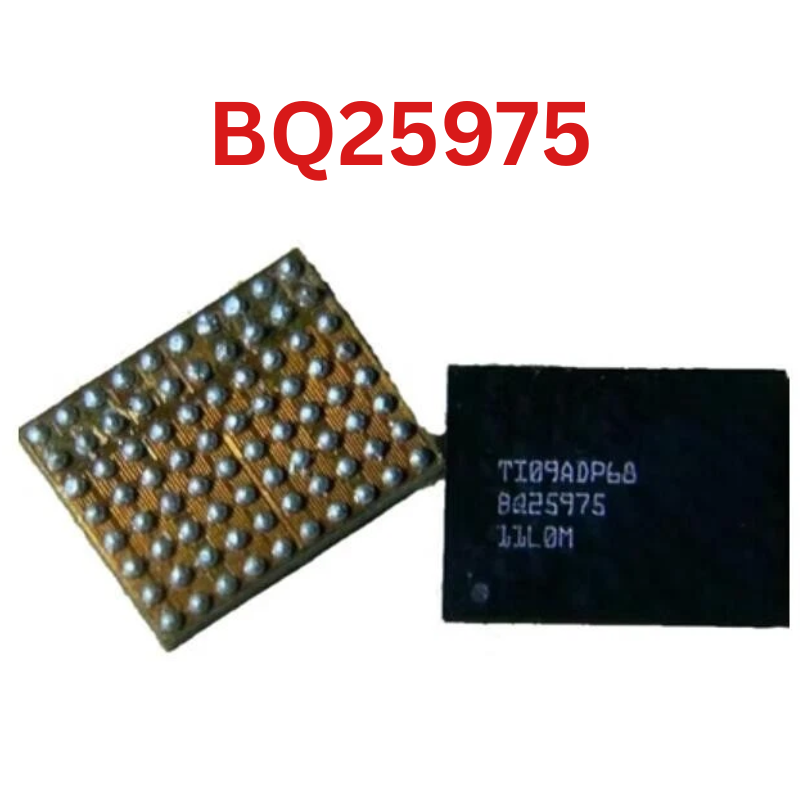
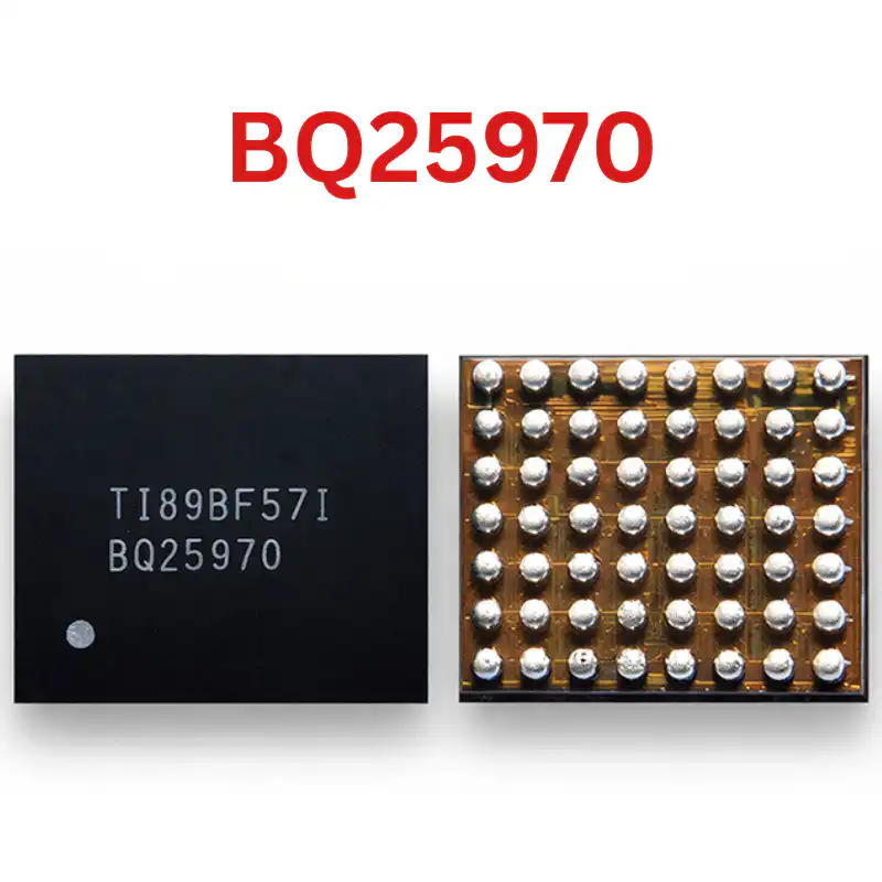
BQ25910 IC
As low as
Rs 0.00
Worldwide shipping · Cash on Delivery
Product Details
1. ARCHITECTURAL OVERVIEW & 3-LEVEL BUCK CONVERTER OPERATION
The Texas Instruments BQ25910 employs a specialized three-level (3L) switching topology:
- 3-Level Topology Advantage: Standard 2-level buck converters switch between VIN and GND, exposing the inductor to large voltage swings (e.g., 9V to 0V). The BQ25910 uses four internal power FETs and an external flying capacitor (CFLY) to create an intermediate switching node at VIN/2.
- Reduced Inductor Size: Because voltage stress across the inductor is cut by 50% and effective ripple frequency is doubled (750 kHz clock produces 1.5 MHz inductor ripple), the required inductance drops from 1.0 µH - 2.2 µH down to 470 nH (0.47 µH). This significantly cuts DCR heat losses and board footprint.
- Parallel / Slave Charging Mode: The BQ25910 operates as a companion/slave fast charger in parallel with a main system PMIC (such as Qualcomm PMI/PM series or TI BQ25890). The main PMIC powers the system rail (VSYS) and handles trickle/pre-charging; once constant-current fast charging begins, the Application Processor enables BQ25910 via I2C to deliver up to 6A directly to the battery.
- Integrated Sensing: Lossless internal current sensing eliminates the need for an external physical current sense resistor, lowering resistance in the battery charging loop.
2. CRITICAL PINS & HARDWARE MEASUREMENTS (36-BALL WCSP)
- VBUS / PMID Balls: Input voltage from USB port (3.9V to 14V). Requires high-voltage ceramic bypass capacitors placed directly adjacent to the die.
- CFLY+ / CFLY- Balls: Flying capacitor terminals connected across the external 10 µF / 16V low-ESR ceramic flying capacitor.
- SW (Switching Node) Balls: Connected to the 470 nH power inductor.
- VBAT Balls: Regulated high-current output routing directly into the battery connector terminal.
- REGN: Internal 5.0V LDO output driving internal gate drivers; requires a 2.2 µF / 4.7 µF decoupling capacitor to GND.
- I2C Control (SDA / SCL): Communicates status, thermal telemetry, and programmable charge parameters to the AP.
- INT / STAT: Open-drain fault indicator and interrupt outputs alerting the host AP of overvoltage, overcurrent, or flying capacitor faults.
3. WORKSHOP DIAGNOSTIC PROCEDURES
- Cold Line Impedance / Diode Mode (Red probe on Ground, Black probe on test point):
* VBUS input: Expected normal drop ~0.500V - 0.600V. (0.000V indicates blown input protection TVS or shorted high-side switching FET).
* VBAT output: Expected normal drop ~0.380V - 0.460V.
* REGN pin: Expected normal drop ~0.500V - 0.580V. (0.000V indicates damaged internal LDO; replace IC).
* SW node: Expected normal drop ~0.400V - 0.500V.
* Flying Capacitor (CFLY): Test both terminals of CFLY relative to ground and across each other. The capacitor must show high resistance across its terminals; a shorted or cracked CFLY will shut down the 3-level switching stage instantly.
- Live Operating Voltage Analysis (Connected to Quick Charge / USB-PD charger):
* Measure VBUS under fast-charge negotiation: Must elevate to 9.0V - 12.0V.
* Measure REGN: Must output steady 5.0V.
* Measure CFLY node: With 9V input, average voltage across CFLY must hold at approximately 4.5V (VIN/2).
* If VBUS remains at 5V and charging current never exceeds 1.5A, communication between the AP and BQ25910 has stalled, or the slave charging circuit has been disabled due to an I2C communication fault.
4. REQUIRED TOOLS & REWORK MATERIALS
- Precision Hot Air Rework Station (Quick 861DW, Atten ST-862D, Sugon 8620DX) with 4 mm - 5 mm nozzle.
- Micro-soldering iron station (JBC C210 or T12) with a micro-chisel or fine knife tip.
- Stereo inspection microscope with LED ring light (minimum 20x to 45x magnification).
- Dedicated 36-ball WCSP / BGA stencil (0.4 mm ball pitch, 0.12 mm thickness).
- Solder alloy: Sn63/Pb37 leaded solder wire (0.2 mm - 0.3 mm) and Sn63/Pb37 solder paste (183°C melting point).
- Consumables: Rosin-based tacky no-clean flux (Amtech NC-559-V2-TF), high-density copper desoldering braid (1.0 mm width), 99.9% pure Isopropyl Alcohol (IPA), high-temperature Kapton tape, aluminum foil heat shield.
5. STEP-BY-STEP REWORK PROTOCOL FOR 36-BALL WCSP
Step 1: Board Clamping & Thermal Shielding
- Secure the logic board into a precision motherboard repair fixture.
- Shield adjacent heat-sensitive components (CPU, UFS/eMMC memory, plastic FPC connectors) with Kapton tape covered by aluminum foil.
- Ensure the battery is disconnected and discharge all remaining energy in input/output capacitors.
Step 2: Desoldering Faulty BQ25910
- Dispense a moderate bead of tacky flux around the perimeter of the 36-ball wafer die.
- Set hot air station to 330°C - 340°C with 35-40 LPM airflow.
- Hold the nozzle vertically (90°) at 1.5 cm distance and circle the chip uniformly for 20 to 25 seconds.
- As the solder balls liquefy, nudge an adjacent passive component to verify melting.
- Lift the bare-die silicon vertically using fine curved tweezers. Never pull or pry against cold solder to avoid ripping fragile 0.4 mm micro-pads from the PCB substrate.
Step 3: PCB Pad Dressing & Planarization
- Apply fresh flux to the logic board pad area.
- Tin the iron tip (set to 340°C) with leaded Sn63/Pb37 solder and sweep across all 36 micro-pads to replace the high-melting-point lead-free factory solder (SAC305).
- Lay fine copper desoldering braid flat over the pads and glide the iron lightly without downward force to remove excess solder until all pads are completely planar.
- Clean thoroughly with 99.9% IPA and an ESD foam swab. Inspect under the microscope for solder bridging or lifted pads.
Step 4: Reballing Replacement BQ25910
- Align the replacement BQ25910 bare die into the matching 36-ball (0.4 mm pitch) stencil under the microscope.
- Spread Sn63/Pb37 solder paste across the 36 apertures, pressing firmly to eliminate air voids. Scrape flush with a clean razor blade.
- Gently dry excess flux with a lint-free wipe.
- Direct hot air at 280°C - 300°C with low airflow (15-20 LPM) from 3 cm distance, moving closer until all paste apertures melt into uniform 0.2 mm - 0.25 mm spheres.
- Allow stencil to cool for 15 seconds, apply a light drop of flux, reflow briefly for 2 seconds to round the balls, and release the IC.
Step 5: Alignment and Reflow Installation
- Apply an ultra-thin, translucent film of tacky flux across the board footprint. Excess flux will float this lightweight bare-die silicon chip out of position.
- Position the BQ25910 onto the footprint, aligning the Pin A1 index dot with the silkscreen indicator on the PCB.
- Apply vertical hot air at 320°C - 330°C with moderate airflow (30-35 LPM).
- As the solder reaches 183°C, the IC will sink and self-align onto the pads via liquid surface tension.
- Execute a delicate "tweezer tap" test: gently tap the corner of the die with tweezers; the chip must immediately bounce back into center alignment.
- Remove heat immediately and allow the board to remain undisturbed.
Step 6: Post-Rework Verification & Testing
- Allow natural cooling for 3 minutes. Never apply cold air or freeze spray, as sudden thermal contraction causes micro-cracking across bare silicon.
- Clean flux residue thoroughly with 99.9% IPA.
- Measure diode mode values across VBUS, VBAT, and CFLY terminals to verify zero solder bridges under the 0.4 mm pitch array.
- Inspect the 470 nH inductor and CFLY ceramic capacitor under magnification for hairline cracks caused by previous thermal events.
- Reassemble the motherboard into the chassis, connect a certified QC/PD fast charger through an inline USB power meter, and verify that fast charging engages with current ramping smoothly up to 3A - 5A+.
You may also like