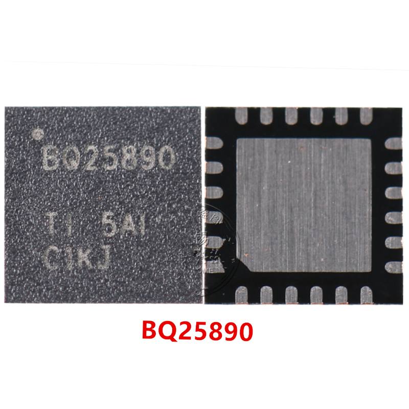
BQ25890 IC
As low as
Rs 0.00
Worldwide shipping · Cash on Delivery
Product Details
1. ARCHITECTURAL & CIRCUIT OVERVIEW
The BQ25890 is an all-in-one switch-mode fast charger and power-path manager. Incoming VBUS passes through internal bi-directional blocking FETs into the PMID pin, feeding an integrated high-side and low-side synchronous buck converter. The switching node (SW, Pins 19/20) drives an external power inductor (typically 1.0uH to 2.2uH) to generate the system rail (SYS, Pins 15/16). An integrated 11 mΩ bidirectional BATFET connects SYS to the battery terminal (BAT, Pins 13/14). D+ and D- pins (Pins 2/3) perform automatic hardware handshake with fast chargers to step up VBUS to 9V or 12V. Digital registers and ADC telemetry are managed by the host processor over I2C (SCL/SDA).
2. CHIP-LEVEL HARDWARE DIAGNOSTICS
A. USB Power Meter Diagnostics:
- 0.00A Static: Check VBUS input fuse / OVP diode. If 5.0V reaches Pin 1 (VBUS) but PMID (Pins 23/24) reads 0V, the internal input FET is blown.
- 0.45A Fixed (Slow Charging): D+/D- lines are open or shorted. The IC defaults to standard USB 500mA limit. Verify 10-ohm inline resistors on D+ and D-.
- Fast Charging Failure: If VBUS stays at 5V instead of negotiating 9V/12V, check DSEL pin and verify that the MaxCharge handshake is enabled in register REG02[0].
B. Cold Diode Mode Measurements (Multimeter in Diode Mode, Red probe on Ground, Black probe on test point):
- Pin 1 (VBUS): Normal drop ~0.500V - 0.600V. (Short <0.050V indicates punctured input ESD suppressor or internal FET short).
- Pins 23/24 (PMID): Normal drop ~0.450V - 0.550V. (Critical: A short on PMID will pull down VBUS and prevent buck operation).
- Pins 15/16 (SYS / Switching Inductor): Normal drop ~0.350V - 0.450V.
- Pins 13/14 (BAT): Normal drop ~0.380V - 0.480V.
- Pins 2 & 3 (D+ / D-): Symmetrical drop ~0.550V - 0.700V.
- Pins 5 & 6 (SCL / SDA): Normal drop ~0.450V - 0.550V.
- Pin 11 (TS - Thermistor input): Normal drop ~0.600V - 0.800V. (If pulled low or open, charger halts charging due to thermal fault).
3. THERMAL MANAGEMENT & PACKAGE PECULIARITIES
- Package Construction: 24-pin WQFN package with perimeter wettable flanks and a large central thermal ground pad (PowerPAD).
- Thermal Sinking: The bottom PowerPAD dissipates heat generated during 5A buck conversion and 9A battery discharge. If the center pad is poorly soldered or lacks solder fill, the IC will rapidly overheat and enter thermal shutdown (TJ > 120°C).
- Surrounding Components: On Xiaomi and Vivo motherboards, the main CPU (Qualcomm Snapdragon / MediaTek Helio), eMMC/UFS memory, and primary PMIC are often within 8mm - 12mm. Shield adjacent silicon using double-layer polyimide (Kapton) tape and aluminum heat-sink foil.
4. STEP-BY-STEP REWORK PROTOCOL
A. Desoldering / Removal:
- Apply a moderate coat of high-grade tacky no-clean RMA flux (e.g., Amtech NC-559-V2 or Kingbo RMA-218) around the QFN package edges.
- Hot Air Rework Station Settings: 330°C - 350°C (depending on station thermal capacity, 6mm nozzle) with 40-45% airflow.
- Pre-heat the entire PCB area from 4cm distance for 20-30 seconds to bring board temperature to ~140°C - 150°C.
- Direct nozzle vertically over the BQ25890 in continuous circular motions. Due to the heavy thermal ground pad, heat transfer requires 25-40 seconds.
- Gently test an adjacent capacitor for solder melt; when molten, lift the QFN package vertically with precision curved tweezers. Do not twist or pull cold ground pads.
B. Motherboard Pad Dressing:
- Apply fresh flux to the 24 perimeter pads and the large central ground slab.
- Using a knife or hoof soldering iron tip at 330°C and copper desoldering braid, wick away old factory lead-free solder until all pads and the center ground plane are completely flat.
- Clean thoroughly with 99.9% anhydrous Isopropyl Alcohol (IPA) and inspect under microscope for broken solder resist webs between pins.
C. Reballing / Tinning:
- Method 1 (Pre-tinning with Iron): Apply a flat, uniform layer of leaded solder (Sn63/Pb37) to the 24 perimeter pins and a thin, level film to the center thermal pad using a micro-chisel tip. Ensure the center pad is not crowned higher than perimeter pins.
- Method 2 (Stencil Reballing): Use a dedicated BQ25890 stencil or universal 0.50mm pitch QFN stencil. Apply Sn63/Pb37 solder paste, wipe clean, and reflow at 260°C with low airflow (15%) to form micro-balls on all pads.
D. Resoldering & Alignment:
- Apply a micro-thin, uniform glaze of tacky flux across the PCB footprint (excess flux under a QFN center pad will boil, causing the IC to float and bridge perimeter pins).
- Align Pin 1 index dot (top-left laser marking) with the PCB silkscreen reference dot.
- Direct hot air vertically at 320°C - 330°C with 30% airflow.
- Watch the perimeter solder joints: As the solder liquefies, the IC will visually self-center on its pads.
- Apply an extremely gentle micro-nudge with tweezers to verify surface tension rebound.
- Remove heat immediately and allow natural cooling for 90 seconds without moving the PCB.
5. POST-REWORK VERIFICATION
- Measure resistance and diode mode value on VBUS, PMID, SYS, and BAT lines to verify zero short circuits to ground.
- Clean residual flux with an ESD brush and IPA.
- Connect battery, plug in an adjustable QC / high-voltage fast charger through an inline USB tester.
- Verify that charging starts immediately, current smoothly ramps to 1.5A - 2.5A+, and VBUS steps up to 9V/12V fast charge mode.
- Verify normal battery percentage accumulation in the Android operating system and confirm USB data syncing (MTP) with a PC.
You may also like