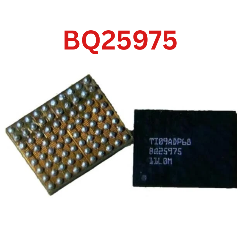
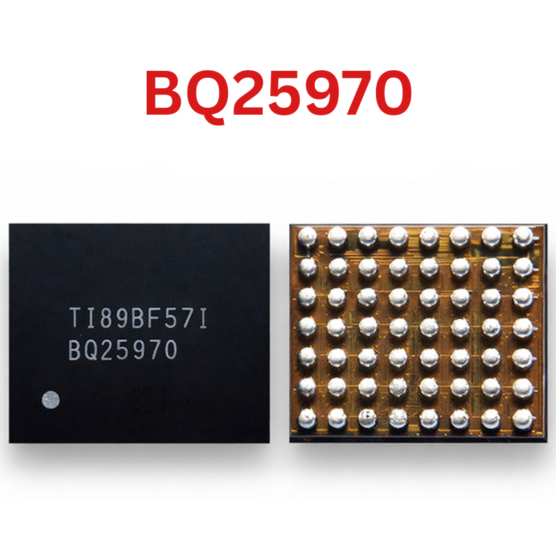
BOT TPA IC
As low as
Rs 0.00
Worldwide shipping · Cash on Delivery
Product Details
1. CIRCUIT ARCHITECTURE & COMPONENT FUNCTION
In smartphone hardware engineering, the label "BOT 7PA" corresponds to two common repair classifications:
Classification A: RF Power Amplifier (PA) Module (Skyworks / RDA 77-series PA)
- Role: Amplifies modulated RF transceiver carrier signals to power levels suitable for over-the-air transmission (+23 dBm to +30 dBm) to cellular base stations.
- Power Supply: Driven directly by battery voltage (V_BATT / VDD_MAIN) or dynamic envelope-tracking voltage from an Envelope Tracking PMIC (ET-IC / APT buck regulator).
- Control Lines: MIPI RFFE (Radio Frequency Front End) serial bus (VIO, SCLK, SDATA) configuring bias levels, band switching, and power modes (High Power / Medium Power / Low Power).
Classification B: Miniature Dual Power Regulator / LDO (TC1302BOT / UM4750-7PA)
- Role: Localized clean voltage distribution delivering isolated analog and digital core voltages for peripheral ICs (image signal processors, camera AF/OIS actuators, sensors).
2. HARDWARE DIAGNOSTICS & FAULT DETECTION
RF Power Amplifier (7PA) Diagnostic Procedure:
- Power Supply Current Analysis (DC Bench Power Supply at 4.0V):
* Baseband VPA Short: If the device shows an immediate high-current short (2A - 5A) before pressing the power button, the RF PA internal GaAs HBT/MOSFET power stage has punched through to ground.
* Transmitter Collapse: If the phone boots normally, displays network bars, but reboots or immediately loses service the moment a phone call is dialed, the PA high-power transmission stage is shorting under transmission load.
- Multimeter Diode Mode Testing (Red probe to Ground, Black probe to test pads):
* Measure V_BATT / VPA supply input line: Normal expected drop is ~0.350V - 0.450V. (0.000V indicates blown internal bypass or damaged transistor array).
* Measure RFFE Clock and Data lines: Typical diode drop is ~0.450V - 0.600V. If one line shows 0.000V or OL, communication with the baseband processor is severed.
Power Regulator (BOT / 7PA) Diagnostic Procedure:
- Measure VIN, VOUT1, and VOUT2 for low-impedance shorts to ground.
- Confirm presence of enable voltage (SHDN / EN ≥ 1.2V) under device operational state.
3. REQUIRED TOOLS & WORKSHOP CONSUMABLES
- Precision Hot Air Rework Station (Quick 861DW, Atten ST-862D, Sugon 8620DX) with 5 mm or 6 mm nozzle.
- Micro-soldering iron station equipped with a chisel or micro-blade tip (JBC C245 / C210).
- Dedicated magnetic or direct-heat BGA/LGA reballing stencil matching the 77-series PA pad footprint.
- Solder alloy: Sn63/Pb37 leaded solder wire (0.3 mm) and Sn63/Pb37 solder paste (183°C melting point).
- Consumables: Rosin-based tacky flux (Amtech NC-559-V2-TF), high-density desoldering wick (1.5 mm - 2.0 mm), 99.9% pure Isopropyl Alcohol (IPA), high-temp Kapton tape, aluminum foil heat shield.
4. STEP-BY-STEP MICRO-SOLDERING REWORK PROTOCOL
Step 1: Board Securing and Heat Shielding
- Fix the motherboard into an adjustable PCB repair clamp.
- Protect adjacent sensitive modules: RF transceiver, Baseband PMIC, and CPU/eMMC/UFS packages must be wrapped in Kapton tape and covered with an aluminum foil thermal shield or copper coin to prevent accidental solder ball bridge ejection.
Step 2: Component Desoldering & Extraction
- Apply a uniform droplet of tacky flux around the perimeter of the IC module.
- Set hot air station to 335°C - 345°C with an airflow rate of 40-45 LPM.
- Heat the component using smooth circular sweeps at a 90° vertical angle, maintaining a distance of 1.5 cm - 2.0 cm for 25 to 35 seconds.
- As the solder reaches the liquidus state, gently nudge a corner with fine curved tweezers.
- Lift the component vertically once all perimeter and center ground pads are liquid. Never pry cold solder to prevent ripping multi-layer RF ground micro-pads.
Step 3: Pad Dressing & Substrate Preparation
- Apply fresh rosin flux over the PCB footprint.
- Set micro-soldering iron to 340°C. Tin the tip with leaded Sn63/Pb37 solder and sweep across the footprint to dissolve the high-melting-point lead-free factory solder (SAC305).
- Lay desoldering wick flat across the footprint. Lightly glide the iron over the wick to absorb excess solder until all pads and center thermal grounds are completely flat.
- Clean thoroughly using 99.9% IPA and ESD foam swabs.
- Inspect under microscope (30x magnification) for torn pads, hairline trace cracks, or exposed copper bridges.
Step 4: Reballing / Pre-Tinning Replacement IC
- For LGA/QFN modules: Place the new IC into the corresponding reballing stencil.
- Apply Sn63/Pb37 solder paste evenly across apertures. Scrape flush with a clean razor blade.
- Heat stencil at 280°C - 300°C with low airflow (15-20 LPM) until uniform, shiny solder spheres form on all pads.
- Allow stencil to cool, apply a light drop of flux, reflow briefly for 2 seconds to round the balls, and release the component.
Step 5: Alignment and Reflow Soldering
- Apply an ultra-thin, translucent film of tacky flux across the logic board footprint.
- Align the component over the board pads using the silkscreen alignment brackets and Pin 1 orientation index dot.
- Direct hot air vertically at 320°C - 330°C with 35 LPM airflow.
- Observe the module sink as the solder reaches 183°C; surface tension will pull the module into alignment.
- Perform a delicate "tweezer tap" test: gently tap the outer corner of the IC body. It must immediately snap back into its original center position, confirming full wetting across all RF and ground pads.
Step 6: Post-Rework Verification & Field Testing
- Allow natural cooling for 3 minutes before handling. Do not force-cool with chemical sprays.
- Clean flux residue thoroughly with 99.9% IPA.
- Measure diode mode on the VPA/V_BATT input to confirm no short circuits exist.
- Reassemble the logic board into the frame, connect antennas and coaxial RF cables securely.
- Insert a functional SIM card, boot the device, place test voice calls on 2G, 3G, and 4G networks, and verify steady RSSI/RSRP signal reception and transmission stability.
You may also like