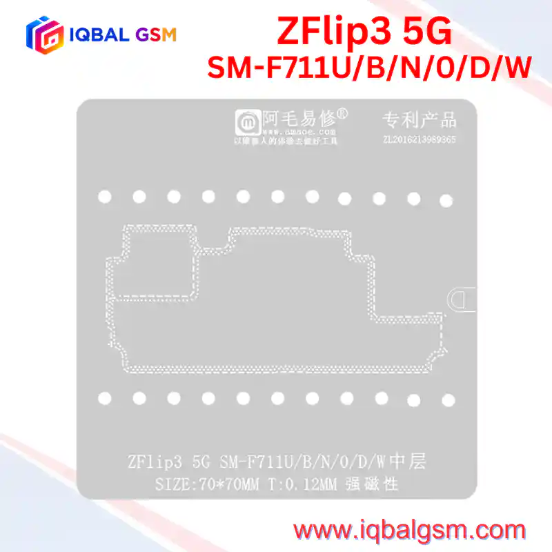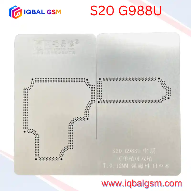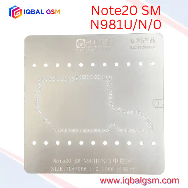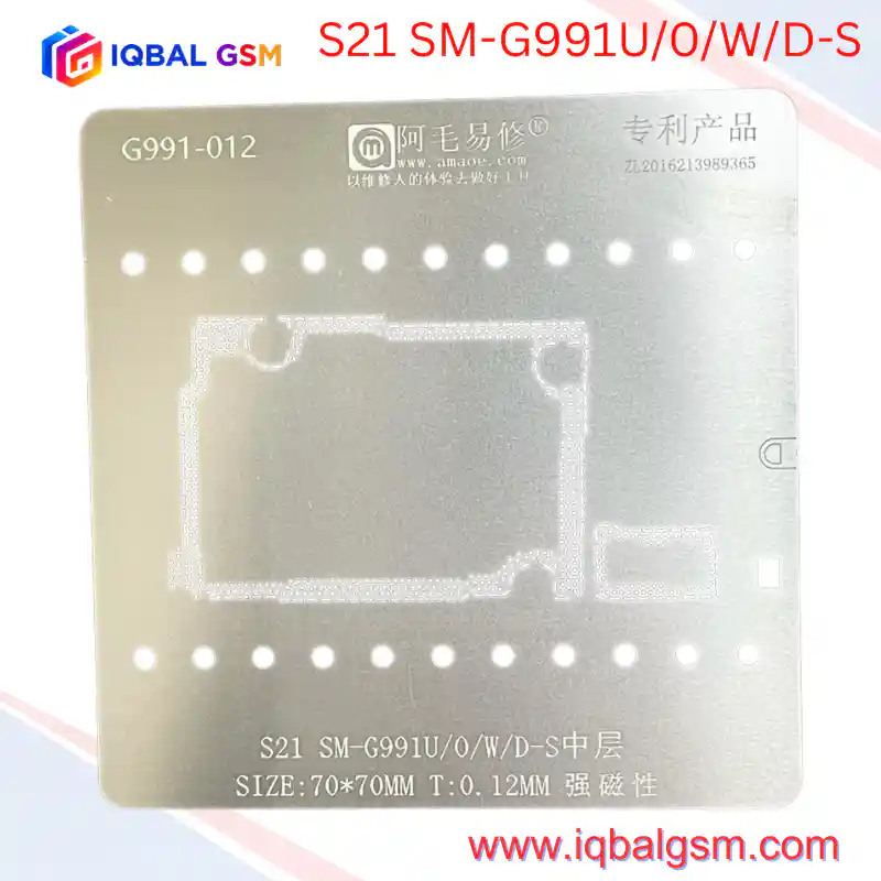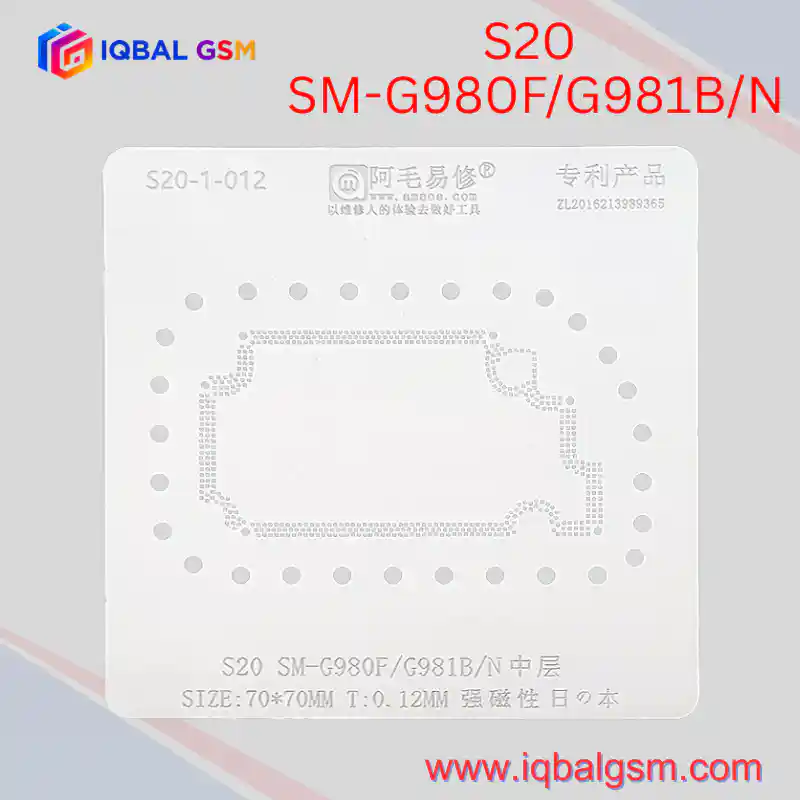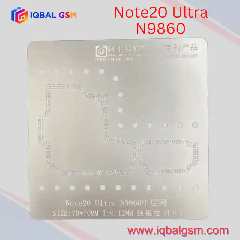

AMAOE S20-3-012 Middle-Layer BGA Reballing Stencil for Samsung Galaxy S20+ (SM-G985F / SM-G986B) – 70x70mm, 0.12mm Strong Magnetic
As low as
Rs 1000.00
Worldwide shipping · Cash on Delivery
Product Details
====================================================================================================
AMAOE S20-3-012 (SM-G985F / SM-G986B) MIDDLE-LAYER BGA STENCIL TECHNICAL REWORK MANUAL
====================================================================================================
1. ARCHITECTURAL PURPOSE & DUAL-LAYER PCB DESIGN
----------------------------------------------------------------------------------------------------
The Samsung Galaxy S20+ International Exynos 990 variants (SM-G985F 4G and SM-G986B 5G) utilize a
vertically stacked dual-layer (sandwich) motherboard architecture to accommodate the 4500mAh battery,
quad-camera array, and 120Hz Dynamic AMOLED 2X display subsystem:
* Lower Board (AP / Core Logic Layer): Houses the Samsung Exynos 990 SoC, LPDDR5 RAM, UFS 3.0 NAND
storage, primary PMICs, and display/charging interfaces.
* Upper Board (RF / Modem / Sub-Layer): Houses the Exynos Modem 5123 (on 5G G986B) or LTE RF
front-end (on 4G G985F), cellular transceivers, power amplifiers, and antenna switches.
* Middle Interposer Frame (中层): A peripheral PCB wall populated with fine-pitch dual-row and
stepped triple-row copper interconnect pads bridging power rails, MIPI lines, RF control signals,
and ground planes between the two stacked PCB halves.
The AMAOE S20-3-012 (70x70mm, 0.12mm thick) strong-magnetic stencil is laser-cut to match the exact
Exynos S20+ interposer footprint, enabling clean solder paste deposition without bridging adjacent pads.
2. KEY STENCIL ENGINEERING SPECIFICATIONS
----------------------------------------------------------------------------------------------------
* 0.12mm Calibrated Thickness: Controls exact solder paste volume per aperture so re-stacked board
halves settle to factory Z-height without cold joints or inter-pad solder bridges.
* Strong Magnetic Alloy (强磁性): Locks firmly onto magnetic reballing jigs and magnetic base plates,
preventing lateral drift during squeegee passes.
* Thermal Warpage Resistance: 70x70mm footprint and high-grade stainless steel composition resist
thermal bowing under direct hot air reflow.
* Exynos Platform Specificity: Engineered specifically for SM-G985F and SM-G986B Exynos 990 boards
(distinct aperture layout from Snapdragon SM-G986U/G988U and base S20 SM-G980F/G981B boards).
3. CRITICAL SIGNALS ROUTED THROUGH THE MIDDLE LAYER
----------------------------------------------------------------------------------------------------
Cracked, oxidized, or bridged solder joints along the S20+ middle interposer typically cause:
* Baseband Unknown / No Service / Emergency Calls Only: Open solder joints on RFFE clock/data,
transceiver IQ lines, or SIM interface lines bridging the AP board to the RF board.
* No Boot / High Standby Current: Squeezed solder balls shorting VPH_PWR / VDD_MAIN rails to adjacent
ground pads during improper board re-stacking.
* Wi-Fi / Bluetooth Grayed Out: Interrupted PCIe/UART control lines or missing 1.8V/3.3V RF power
rails across the interposer perimeter.
* Display / Camera / Charging Faults: Broken MIPI, I2C, or USB differential lines routed through the
lower-right tail section of the interposer.
4. STEP-BY-STEP MIDDLE-LAYER REBALLING & RE-STACKING WORKFLOW
----------------------------------------------------------------------------------------------------
A. BOARD SEPARATION & PAD PREPARATION:
1. Place the SM-G985F / SM-G986B motherboard onto a dedicated pre-heating platform set to 175°C–190°C.
2. Once the factory middle-layer solder reaches liquidus, lift the upper RF board vertically using
curved ESD tweezers without applying sideways shear force.
3. Sweep both upper and lower interposer rings with a wide knife-edge soldering iron tip (320°C),
low-melt solder (138°C Bi/Sn alloy), and tacky flux to lower residual lead-free solder melting point.
4. Clean all interposer pads thoroughly with 0.8mm/1.0mm desoldering wick and 99.9% Isopropyl
Alcohol (IPA) until every pad is flat and mirror-bright.
B. STENCIL ALIGNMENT & SOLDER PASTE APPLICATION:
1. Seat the lower/middle-layer PCB onto a magnetic S20+ reballing fixture or flat silicone pad.
2. Position the AMAOE S20-3-012 stencil over the board, aligning the stepped perimeter aperture ring
precisely with the PCB copper pads under a stereo microscope.
3. Apply 183°C Sn63/Pb37 (or 158°C/138°C medium-temp) solder paste across the stencil using a
stiff stainless scraper at a 45-degree angle in one smooth pass.
4. Hold the stencil flat and heat evenly with a hot air gun at 260°C–280°C (low airflow, nozzle
~2cm away) until all paste converts into uniform silver solder spheres, OR lift the stencil
vertically first and reflow the printed paste directly on the board.
5. Inspect every perimeter solder ball under the microscope for uniform height and zero bridges.
C. BOARD RE-STACKING (REJOINING):
1. Apply a thin film of no-clean tacky flux along the opposing board's clean interposer pads.
2. Align the upper and lower halves accurately on the pre-heating platform.
3. Heat at 185°C–195°C (matching the chosen solder alloy) until the upper board settles naturally
by surface tension (apply a gentle 1mm nudge with tweezers to confirm self-centering).
4. Allow the board to cool naturally to room temperature before testing with a DC bench power
supply for shorts on VPH_PWR / VDD_MAIN.
5. POST-REWORK VERIFICATION & BENCH DIAGNOSTICS
----------------------------------------------------------------------------------------------------
* Diode Mode Check: Probe key connector lines (SIM, Display, Charging, RF) in diode mode before
powering on to verify zero open lines (OL) or dead shorts to ground.
* DC Power Supply Boot Test: Connect to a regulated 4.2V DC bench supply; verify zero pre-boot
leakage current and clean boot current progression.
* Full RF & Connectivity Audit: Confirm 4G/5G signal registration, Wi-Fi/Bluetooth MAC address
presence, NFC, and 120Hz Dynamic AMOLED 2X display output.
====================================================================================================
You may also like