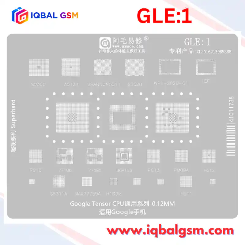

U-GGE1
As low as
Rs 700.00
Worldwide shipping · Cash on Delivery
Product Details
================================================================================
1. GENERATIONAL SILICON & BGA SUBSTRATE OVERVIEW (U-GGE1)
================================================================================
The AMAOE U-GGE1 stencil is an all-in-one CPU/RAM master template engineered specifically
for mobile board technicians performing Tier-3/Tier-4 motherboard swaps, CPU transfers, and
dead-boot reballing across all five generations of Google Tensor silicon:
A. TENSOR G1 (GS101 / S5P9845) — APERTURES (7) & (8):
- Co-developed with Samsung System LSI; manufactured on Samsung 5LPE (SF5E).
- Package Architecture: FOPLP-PoP (Fan-Out Panel Level Package - Package-on-Package).
- Ball Pitch & Count: 0.35 mm pitch with center decoupling ground array.
- Dual Apertures: Aperture (7) matches the primary 0010310614 production substrate;
Aperture (8) accommodates secondary/alternate substrate revisions used on Pixel 6a.
B. TENSOR G2 (GS201 / S5P9855) — APERTURE (3):
- Samsung 5nm process node. Refined BGA ballout with modified central bypass capacitor
keep-out cutouts to reduce parasitic inductance for the 7-core Mali-G710 MP7 GPU.
- Used in Pixel 7, Pixel 7 Pro, Pixel 7a, Pixel Fold, and Pixel Tablet.
C. TENSOR G3 (GS301 / S5P9865) — APERTURE (2):
- Samsung SF4 (4nm) process node. Introduces a 9-core CPU topology (Cortex-X3, A715, A510).
- Substrate Layout: Highly congested center ground grid surrounded by high-speed memory
and system-bus balls. Utilizes iPoP on Pixel 8a and FOPLP-PoP on Pixel 8 / 8 Pro.
D. TENSOR G4 (GS401 / S5P9875) — APERTURES (5) & (6):
- Samsung SF4P process node with redesigned thermal dissipation architecture.
- Dual Footprint Substrates on U-GGE1:
* Aperture (5) [G4-F1KZ1Y04]: Engineered for the flagship FOPLP-PoP package on Pixel 9,
Pixel 9 Pro, Pixel 9 Pro XL, and Pixel 9 Pro Fold.
* Aperture (6) [G4-P050510513]: Engineered for the alternate packaging variation (iPoP)
utilized in the Pixel 9a tier to reduce manufacturing thickness and cost.
E. TENSOR G5 (G313-09488-00) — APERTURE (1):
- Completely independent custom Google design manufactured on TSMC 3nm (N3E).
- Breakthrough Substrate Layout: Features dual side-rail perimeter contact arrays
optimized for TSMC advanced packaging, Imagination PowerVR GPU interconnects,
and next-generation low-latency bus routing for the Pixel 10 series.
F. RAM 496 (POp UPPER MEMORY) — APERTURE (4):
- Universal JEDEC 496-ball perimeter interposer footprint.
- Directly reballs the top-tier 8GB, 12GB, and 16GB LPDDR5 / LPDDR5X SDRAM packages
(Micron, Samsung, SK Hynix) that stack atop Tensor G1, G2, G3, and G4 base SoCs.
================================================================================
2. SOLDER ALLOY SELECTION & TEMPERATURE PROFILES
================================================================================
The 0.12 mm thickness of U-GGE1 provides the exact solder volume required for fine-pitch
(0.35 mm - 0.40 mm) Google Tensor balls. Utilizing the wrong alloy will cause intermediate
joint collapse or popcorning:
- Lower Tier (Base Tensor SoC to Motherboard):
* Primary Choice: Sn63/Pb37 Leaded Solder Paste (Melting Point: 183°C, Type 4 or Type 5 mesh).
* Lead-Free Choice: Sn96.5/Ag3.0/Cu0.5 SAC305 (Melting Point: 217°C).
- Upper Tier (LPDDR5/5X RAM 496 onto Tensor SoC Interposer):
* MANDATORY Dual-Temperature Strategy: Use Sn42/Bi58 Low-Melt Paste (Melting Point: 138°C) or
Sn62/Pb36/Ag2 (Melting Point: 179°C).
* Critical Rule: The upper RAM solder must melt 15°C to 45°C BELOW the lower SoC solder.
If the same 183°C alloy is used on both tiers, installing the RAM will remelt the SoC
base balls, causing bridging under the CPU weight.
================================================================================
3. COMPREHENSIVE REWORK & REBALLING WORKFLOW
================================================================================
PHASE 1: CHIP REMOVAL & POP SEPARATION
1. Secure the motherboard in a dedicated CNC/magnetic repair fixture. Mask peripheral components,
FPC connectors, and cameras using multi-layer thermal kapton and aluminum foil tape.
2. Bottom Pre-Heat: Apply bottom heating at 150°C - 165°C across the board underside.
3. Top Airflow: Apply 355°C - 365°C hot air (40% - 50% flow, 8 mm - 10 mm nozzle) in smooth,
concentric rectangles over the LPDDR5 RAM.
4. Using an ultra-thin 0.06 mm separation pry blade, slice the softened perimeter glue and lift
the RAM off the upper SoC interposer ring.
5. Immediately reheat the base Tensor SoC to 365°C and lift it from the motherboard pads.
PHASE 2: UNDERFILL REMOVAL & RESURFACING
1. Lower hot air to 250°C. Apply moderate rosin-based flux and gently remove residual black
epoxy underfill using a specialized non-scratch copper scraper blade.
2. Apply fresh leaded solder (183°C) to the PCB pads and IC bottom using a C210 micro-soldering
iron with a bevel/knife tip (325°C).
3. Level with ultra-fine desoldering wick until all pads are uniform and flat. Clean with pure IPA.
PHASE 3: REBALLING WITH THE AMAOE U-GGE1 STENCIL
1. Seat the Tensor IC or RAM into a reballing magnetic base or flat silicone mat.
2. Match the chip to its exact labeled aperture (1 through 8). Ensure the anti-bulging vent
holes align over the substrate's outer edges.
3. Squeegee paste across the holes at a 45° angle. Scrape off all surface residue with a clean blade.
4. Hot-Air Reballing:
- Set hot air to 310°C - 325°C with low airflow (25% - 30%) to prevent paste spatter.
- Heat gradually from the outside perimeter inwards. Solder spheres will form simultaneously.
- Let cool for 8-10 seconds before lifting the stencil vertically.
- Apply a drop of liquid flux and give a 3-second reflow at 320°C to ensure perfect ball roundness.
PHASE 4: TWO-STEP POP RE-INSTALLATION
1. Step 1 (SoC to Motherboard):
- Apply a microscopic layer of tacky RMA flux to the PCB pads (excess flux causes chip drift).
- Align the Tensor SoC to motherboard corner silkscreen markers.
- Reflow with top air at 345°C - 355°C (bottom preheat at 150°C). When surface tension centers
the chip, verify with a gentle 0.1 mm tweezer nudge test.
2. Step 2 (RAM 496 to SoC):
- Allow the board to cool to room temperature.
- Apply a micro-layer of low-viscosity flux across the upper SoC PoP contact ring.
- Align the reballed RAM 496 (Pin 1 dot aligned to SoC Pin 1).
- Reflow using low temperature (240°C - 260°C for 138°C paste, or 310°C for 179°C paste)
with low airflow (25%). The lower SoC solder joints remain completely solid and undisturbed.
================================================================================
4. ELECTRICAL DIAGNOSTICS & FAULT MATRIX
================================================================================
- Diode Mode Impedance Values (Red probe to Ground, Black probe to test points):
* VDD_CORE / VDD_CPU / VDD_TPU / VDD_GPU : 0.008 V - 0.045 V (Normal low-impedance state).
* VDD_MEM / LPDDR5 VDD1 / VDD2H / VDDQ : 0.280 V - 0.420 V (Normal).
* VSYS / Primary Battery Line : 0.420 V - 0.530 V (Short < 0.050 V indicates PMIC/SoC bridge).
- DC Power Supply Current Behavior (4.2V VBAT):
* 0 mA (Pre-Power) -> Normal standby.
* 30 mA - 60 mA (Fixed upon trigger) -> Primary PMIC failure, missing 38.4 MHz clock, or SoC cold joint.
* 90 mA - 160 mA (Jumping/Cycling) -> CPU initialized; RAM 496 open circuit, missing VDDQ, or UFS NAND fault.
* 200 mA -> 600 mA -> 1.2 A+ -> Successful boot into Android OS.
You may also like