
GLE-1
As low as
Rs 700.00
Worldwide shipping · Cash on Delivery
Product Details
================================================================================
1. ARCHITECTURAL OVERVIEW & CHIP-LEVEL ECOSYSTEM (GOOGLE TENSOR G1 / G2)
================================================================================
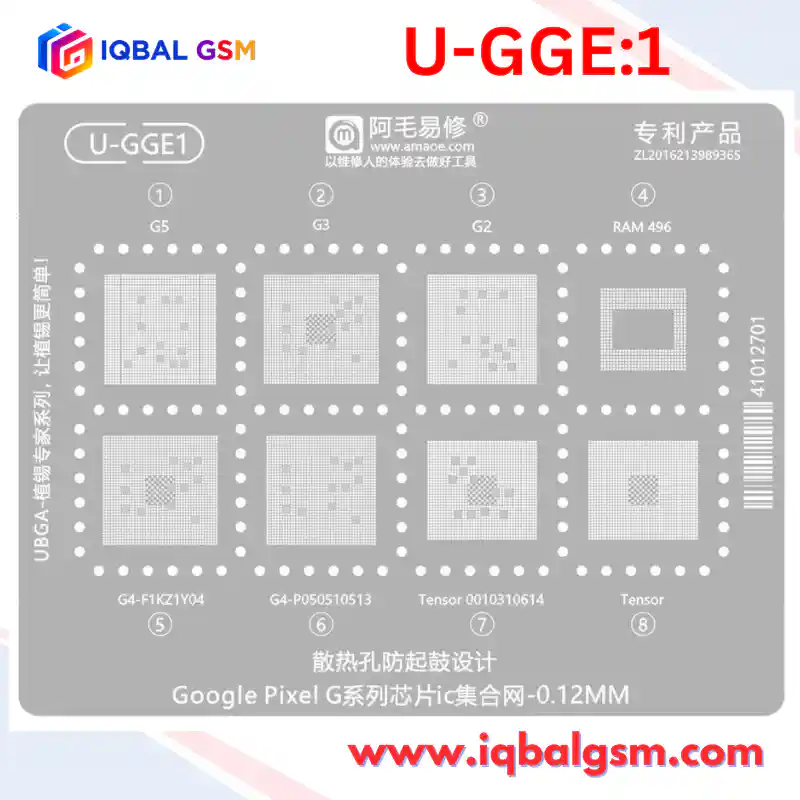
The AMAOE GLE:1 (0.12 mm) stencil is a comprehensive board-level rework template
engineered for Google's first- and second-generation custom silicon platforms co-developed
with Samsung System LSI:
A. APPLICATION PROCESSORS & POP MEMORY (MIDDLE ROW):
- Google Tensor G1 (Part #: GS101 / Die Mark: S5P9845, Codename "Whitechapel"):
* Process & Die: Samsung 5nm LPE (SF5E), 10.38 mm x 10.43 mm (108.26 mm2).
* CPU Cluster: 2x Cortex-X1 @ 2.80 GHz + 2x Cortex-A76 @ 2.25 GHz + 4x Cortex-A55 @ 1.80 GHz.
* GPU & AI: 20-core Arm Mali-G78 MP20 + 1st-Gen Google Edge TPU ("Abrolhos").
* Packaging: FOPLP-PoP (Fan-Out Panel Level Package - Package-on-Package) with 4-channel
16-bit LPDDR5-6400 SDRAM (8 GB on Pixel 6, 12 GB Micron MT62F1536M64D8CH-031 WT:A on 6 Pro)
mounted directly atop the SoC interposer ring.
- Google Tensor G2 (Part #: GS201 / Die Mark: S5P9855, Codename "Cloudripper"):
* Process: Samsung 5nm (SF5E), FOPLP-PoP (Pixel 7 / 7 Pro) and iPoP (Pixel 7a).
* CPU Cluster: 2x Cortex-X1 @ 2.85 GHz + 2x Cortex-A78 @ 2.35 GHz + 4x Cortex-A55 @ 1.80 GHz.
* GPU & AI: 7-core Arm Mali-G710 MP7 + 2nd-Gen Edge TPU ("Janeiro") + GXP DSP.
* Footprints: Uses the right-side large BGA aperture featuring asymmetric center keep-out
islands for backside decoupling capacitors and ground planes.
B. POWER MANAGEMENT ARCHITECTURE (PG10 / PG11 / PG12 / PG13 / MAX77759A):
- Master & Slave Core PMICs:
* Pixel 6 / 6 Pro uses dual Samsung PMICs: S2MPG10 (Master PMIC - supplies VDD_CPU_CL0/CL1/CL2,
VDD_TPU, VDD_INT, and RTC rails) + S2MPG11 (Slave PMIC - supplies VDD_G3D, LPDDR5 rails
VDD1/VDD2H/VDDQ, camera LDOs, and display power).
* Pixel 7 / 7 Pro upgrades this pair to S2MPG12 (Master PMIC, stencil label "PG12") +
S2MPG13 (Slave PMIC, stencil label "PG13").
- Companion IF & Charger PMIC (MAX77759A / MAX77759AEWN+):
* High-density Wafer-Level Package (WLP) managing USB Type-C PD / TCPC, primary buck-boost
system rail (VSYS) generation, battery charging coordination with NXP PCA9468 switched-capacitor
direct charger, and Max1720x fuel gauge telemetry.
- Security Processor (H1D3M - Google Titan M2):
* Standalone RISC-V secure element communicating with the Tensor SoC over dedicated SPI lines.
Crucial Note: H1D3M is cryptographically paired to the board's provisioning state; always
preserve and reball the original H1D3M during board swaps or dead-boot recovery.
C. BASEBAND MODEM & RF FRONT-END SUBSYSTEM:
- External 5G Modems: Neither GS101 nor GS201 integrates a cellular baseband on-die (on Pixel 6/6 Pro;
GS201 pairs with S5300).
* A5123 (Samsung Exynos Modem 5123): Standalone 5G Sub-6/mmWave baseband on Pixel 6 / 6 Pro,
powered by dedicated modem PMIC S5311A and paired with SHANNON5511 (S5M5511) RF Transceiver.
* S5300 (Samsung Exynos Modem 5300): Standalone/paired 5G baseband on Pixel 7 / 7 Pro, powered
by S2MPM09A ("PM09A") and paired with S5520 RF Transceiver.
- RF Front-End LGA Modules (77080 & 77180):
* Hybrid LGA/BGA pad layouts with large central thermal/ground slugs and perimeter signal pads.
================================================================================
2. SOLDER PASTE & THERMAL GRADIENT STRATEGY
================================================================================
Because the AMAOE GLE:1 stencil is 0.12 mm thick, aperture paste volume is optimized for fine-pitch
0.35 mm - 0.40 mm CPU/PMIC pads without bridging adjacent ground/power balls:
- Bottom Layer (Tensor GS101 / GS201 SoC Base, BGA153 UFS, S2MPG10/11/12/13, A5123/S5300):
* Recommended Paste: Medium-Temperature Sn63/Pb37 (183°C) for standard repair, or Sn96.5/Ag3.0/Cu0.5
SAC305 (217°C) if matching factory lead-free profile.
- Upper PoP Layer (LPDDR5 RAM over Tensor SoC - Center Stencil Aperture):
* Recommended Paste: Low/Medium-Temperature Sn42/Bi58 (138°C) or Sn62/Pb36/Ag2 (179°C) T4/T5 mesh
solder paste to prevent lower SoC BGA balls from secondary remelting and blooming during PoP
RAM installation.
- RF Shielded LGA Modules (QM77080 / 77180):
* Recommended Paste: 138°C / 158°C low-melt or 183°C leaded paste to avoid delaminating internal
RF module substrate dies.
================================================================================
3. STEP-BY-STEP TENSOR CPU PoP & PMIC REWORK PROCEDURE
================================================================================
STEP 1: PRE-BAKING & BOARD PREPARATION
- Bake the Pixel 6 Pro / Pixel 7 Pro logic board at 110°C for 30-45 minutes if moisture exposure is
suspected (FOPLP-PoP packages on GS101/GS201 are highly prone to "popcorning" and substrate
warpage if heated rapidly with trapped moisture).
- Mount the logic board in a dedicated high-mass PCB holder. Place heat-reflective aluminum tape
over the plastic display/FPC connectors, microphone ports, and optical camera sensor housings.
STEP 2: SEPARATING & DESOLDERING THE TENSOR PoP STACK
- Apply tacky flux around the perimeter of the LPDDR5 RAM (top tier of the Tensor PoP).
- Using a precision hot-air station (e.g., Quick 861DW / JBC):
* Pre-heat the board on a bottom preheater at 140°C - 160°C.
* Set hot air to 350°C - 365°C, airflow 45% - 55% (spiral motion around the RAM perimeter).
* Slide a 0.06 mm - 0.08 mm polished separation blade into the corner interposer gap to lift the
LPDDR5 RAM off the Tensor SoC without stressing the thin SoC die underneath.
* Immediately lift the lower Tensor SoC (GS101 or GS201) while the underfill is soft at ~365°C.
STEP 3: PAD CLEANING & UNDERFILL REMOVAL
- Lower hot-air temperature to 250°C - 260°C and use a curved hook blade (#11 or #27) to gently
scrape softened black epoxy underfill from both the PCB pads and the IC package substrate.
- Apply 138°C low-melt solder with a temperature-controlled micro-soldering iron (320°C - 340°C,
C210 knife/bevel tip) and desoldering braid (wick) to level all BGA pads on the Tensor SoC,
LPDDR5 RAM, and motherboard without scraping the solder mask.
- Clean thoroughly with 99.9% Isopropyl Alcohol (IPA) or PCB flux remover until mirror-flat.
Inspect under a stereo microscope (20x-40x) and repair any torn NC/signal pads with 0.01 mm
insulated copper jump wire and UV-curable green solder mask.
STEP 4: REBALLING WITH THE AMAOE GLE:1 (0.12mm) STENCIL
- Place a lint-free Kimwipe or heat-resistant magnetic base beneath the cleaned IC (GS101/GS201,
LPDDR5 RAM, MAX77759A, or S2MPG10/12).
- Align the corresponding aperture on the AMAOE GLE:1 0.12mm stencil over the IC pads. The circular
vent holes surrounding the three central Tensor apertures prevent stencil bowing during heating.
- Spread a uniform layer of fresh, dry-consistency 183°C solder paste across the apertures using a
flexible steel squeegee at a 45° angle. Wipe the stencil surface completely clean of excess beads.
- Hold the stencil down firmly with bent-tip titanium tweezers across the bridge zones, and reflow
with hot air at 310°C - 330°C (airflow 30%) from the outer perimeter inward until all solder balls
coalesce into uniform spheres.
- Allow 10 seconds to cool and solidify before lifting the stencil, then apply a drop of fresh flux
and perform a 3-second touch-up reflow so every ball centers on its pad.
STEP 5: REFLOW INSTALLATION (TWO-STAGE OR COMBINED PoP)
- Method A (Recommended - Two-Stage Sequential Reflow):
1. Apply a micro-thin film of tacky flux to the motherboard CPU pads (wipe off excess so the chip
does not float).
2. Align the reballed Tensor SoC (GS101/GS201) to the board corner fiducials and reflow at 340°C -
355°C (airflow 45%) until surface tension pulls the SoC into alignment (verify with a gentle
0.2 mm tweezer nudge test).
3. Let the board cool, clean the top interposer ring of the installed Tensor SoC, apply a minimal
film of flux to the PoP ring, align the reballed LPDDR5 DRAM (Pin 1 dot matched to SoC Pin 1),
and reflow at 320°C - 335°C.
================================================================================
4. POST-REWORK DIAGNOSTIC & BOOT VERIFICATION CHECKLIST
================================================================================
1. Diode-Mode Impedance Check (Cold Board):
- Measure VSYS (Main Power Rail around MAX77759A coils) and main buck inductors around S2MPG10/12.
- Note: Tensor CPU/GPU core rails (VDD_CPU_CL0/CL1, VDD_G3D, VDD_TPU) naturally exhibit very low
ohmic resistance (8 Ohms - 35 Ohms), which is normal and NOT a short circuit. A dead short on
1.8V_AP or VSYS (< 2 Ohms) indicates a bridged ball under the PMIC or SoC.
2. DC Bench Power Supply Current Draw Sequence (4.2V Input):
- Pre-Trigger Standby: 0.000 A (Zero leakage current prior to pressing Power).
- Post-Trigger Boot Sequence:
* Stuck at 45 mA - 75 mA (Fixed): Indicates failed PMIC sequencing (check S2MPG10/11/12/13 or
missing 38.4 MHz crystal clock).
* Cycling 90 mA -> 140 mA -> 0 mA (Bootloop / DFU): Indicates LPDDR5 PoP upper layer open/bridged
joint or UFS BGA153 communication fault. Re-seat or reball the LPDDR5 RAM using the center
GLE:1 aperture.
* Normal Boot: Steps steadily from 120 mA -> 350 mA -> 800 mA -> 1.4 A+ as Google logo loads.
3. Baseband & IMEI Verification:
- After OS boot, dial *#06# to confirm IMEI presence. If Baseband shows "Unknown", inspect the
A5123 / S5300 modem and S5311A / S2MPM09A modem PMIC rails.
You may also like